Oscilloscope Current Measurement on the Cheap
I have been spending a lot of time working on microcontroller power optimisation recently, and not having a current probe for my oscilloscope has been quite inconvenient. Working with current optimisation without a current probe is like designing a circuit without an oscilloscope – shooting in the dark.
Can I Just Buy Something?
Yes, but commercial current probes are very expensive and unwieldy. For example, this is (as far as I can tell) the lowest end current probe from Rigol (known for extremely cheap test equipment):
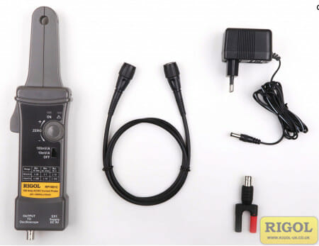
Rigol RP1001C
It’s a hall effect probe to be clamped around a conductor, and requires a separate power supply. All for the bargain basement price of £791 (~US$1000), which is a bit more than double what I paid for my oscilloscope! It’s also very bulky and requires its own power supply.
Now if you need the specs they offer (100A peak, 300 kHz bandwidth, and no voltage drop), that’s probably the way to go.
But my requirements are much more modest – I only realistically need up to 10A (<1A 99% of the time), 10 kHz, and don’t mind a reasonably small burden voltage since the boards I work with all have onboard regulators anyways.
So I set out to build something that is at least an order of magnitude cheaper, and also an order of magnitude smaller.
The Theory
The general idea of a shunt-based current sensor is very simple:
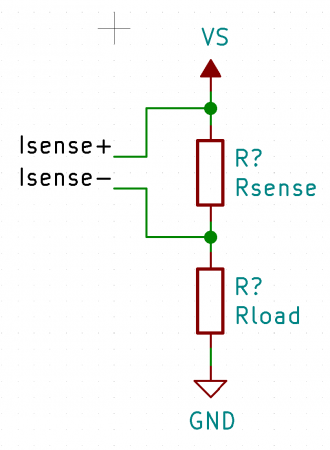
Shunt current sensor
We put a resistor in series with the load, and measure voltage drop across the resistor, and use V = IR to work out current through the resistor (and therefore the load). Nice and simple, but two problems:
- We want (Isense+ – Isense-) to be large so we can make a low noise measurement, but that means we have a high voltage drop to the load that depends on the current (basically we are increasing the source resistance of the power supply), which we want to minimise. The voltage drop due to current measurement device is called burden voltage.
- The voltages are on the +Vs side, which are hard to measure (this is called high-side sensing). Why not have the sensing resistor between the load and ground? It’s possible, but if the load is a circuit that needs to communicate with another circuit referenced to the same ground, we really don’t want to “lift” the ground when the load draws current, which would be the case here. That’s why the vast majority of applications use high side sensing. Generally supply voltage dropping is less of a problem for circuits than ground rising.
The solution is to use a differential amplifier to amplify the voltage across Rsense, and output an amplified voltage difference relative to ground. This solves both problems – the amplification allows us to use a very small Rsense and have a very small voltage drop, while still getting a large sense voltage for measurements, and shifting the sense voltage to be relative to ground makes it easier to measure.
Component Choices
This is a very common application, so although you can use a generic differential amplifier (or instrumentation amplifier), there are many products designed and optimised specifically for this use, with most of the necessary external components integrated into the chip, usually sold as “current-shunt monitors/amplifiers”, and it’s a good idea to use them. I chose the Texas Instruments INA213 current shunt monitor, because it’s cheap (US$0.587 each from JLC), has a very low offset voltage (Voff) of ±35 µV, which allows me to minimise the burden voltage by using a very small shunt resistor. There are also versions with high precision integrated ADC with digital (either I2C or SPI) output, and they are good choices if you are integrating current sensing into your microcontroller project, but since we are reading with an oscilloscope, we will go with a standard voltage output device.
Voff can be thought of as a voltage error on the input. The larger the Voff, the larger the Rsense we need, to maintain the same signal-to-noise ratio (SNR). Therefore, Voff is one of the most important parameters for a differential amplifier.
The INA21x series comes in many different gain options from 50 to 1000. Generally, higher gains allow the use of a smaller resistance and hence lower burden voltage, but increases noise, and decreases bandwidth, since amplifier bandwidth is usually inversely proportional to gain – see Gain-bandwidth product%20and%20vice%20versa.). That is the case here as well. The 50x gain version I chose has an advertised bandwidth of 80 kHz typical, whereas the 1000x version has a bandwidth of 4 kHz. I chose 50x gain because bandwidth is more important to me than burden voltage, which is already low enough at 50x, which would give me a 1V output from a 20 mV burden voltage. My circuits don’t usually care about anything as small as 20 mV.
The INA21x series can also be powered by anything from 2.7V to 26V, which covers all the supply voltages I use. That means I can make the setup simpler by trading flexibility for convenience and just power the amplifier from my power supply.
Circuit Design
Here is the circuit design:
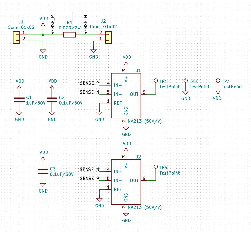
Schematics
Pretty straight forward. I am using a 20 mΩ resistor, so that at a maximum current of 10A, I get a voltage of 200mV, which amplifies to 10V, giving us a nice 1 V/A relationship on the output. 10A ^ 2 * 20 mΩ = 2W, so I got a 2W rated resistor.
I used two INA213 devices because I want to be able to measure both positive and negative currents (eg. during motor flyback), so they are wired identically, with just SENSE_N and SENSE_P swapped. This is technically not necessary – if you look at the datasheet, it says the device is capable of bi-directional measurements. The way that works is by wiring REF to (usually) Vdd/2, so if the output voltage is higher than Vdd/2, it’s positive, and vice versa. I didn’t want to do that because that would make it harder to read oscilloscope output, and also harder to get the oscilloscope’s variable gain amplifier to amplify small outputs (since they always amplify relative to ground). The INA213 only costs US$0.587 each, so the easiest solution is to just use two amplifiers. Where a unified trace is needed, I can probe both, and use MATH function on the scope to take the difference. That does require the use of two channels – I am not too worried about that because I have a 4 channel scope. If you want to save a channel, you can also build some additional circuit (eg. charge pump inverter) to generate a negative supply, and power the INA213 with +Vs and -Vs, with REF tied to ground. I thought about doing that, but it would reduce maximum supply voltage to 13V, and having 26V supply range is more important to me. Of course, you can also add a regulator, but then your minimum supply voltage will go up from 2.7V, due to regulator dropout, and I really want to support 3.3V supply, which makes it difficult. At the end of the day, this is an extremely cheap device, and I can always make another one with different design decisions should it become necessary.
PCB Design and Gotchas
PCB design
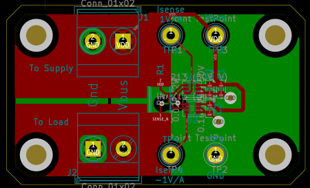
PCB design is the hardest part of this project. We are working with very low voltages, so we need to pay a lot of attention to minimising noise. I have the input and output connectors on the left, Rsense and the two amplifiers on the right, with the outputs brought out to test terminal posts for easy probing. I also have ground and Vsupply broken out into test terminals. Ground is especially important – for precise measurements we always want to ground the probe as close as possible to the test point.
Let’s talk about ground first. This is the ground plane:
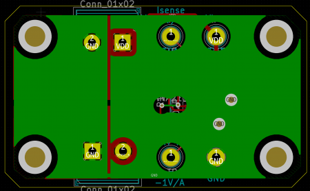
Ground plane
The entire back layer is ground, but I have a thin slot splitting it down the middle, only connected at a tiny point at the bottom. This way the left side is used by the load (I want a very low impedance connection from input ground to output ground), and the right side is ground for the amplifiers. It’s important to split them to ensure that load return current doesn’t go under the amplifiers, because that would lift the amplifier ground, and load transients may inductively couple to amplifier signals. Not something we want for precise measurements! This is called star grounding topography. Altium has a very nice article on this for further reading.
Now back to the front side:
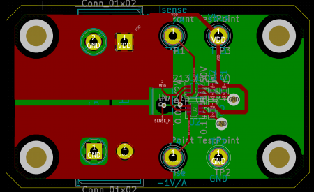
Front side
Here we have two copper pours to connect input supply voltage to Rsense, and from Rsense to output supply voltage. Why pours? Because we want very low impedance paths, as well as provide some heatsinking for Rsense, which will get very hot if we do actually push 10A through it! But again, I don’t want to go over to the amplifier side, due to potential for introducing noise.
Note that the amplifiers are connected to Rsense using the Kelvin sensing technique. This is very important when we are amplifying voltages across tiny resistances like what we have here. We have to ensure that the load current isn’t going to flow through any part of the trace connecting amplifiers to the resistor pads. A Kelvin connection ensures that.
That is it for the PCB!
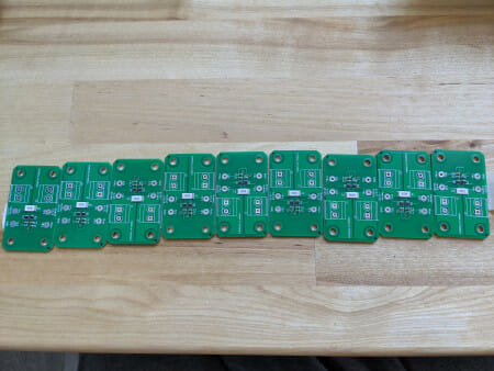
Getting It Made!
I have the PCB manufactured and (mostly) assembled by JLCPCB, who has been amazing and I can totally recommend.
Full disclosure: JLCPCB is generously sponsoring my projects, but I was already a big fan of them before they reached out, and I would never recommend a company that I wouldn’t use if I had to pay myself.
If you are wondering how to use their SMT assembly service with KiCad, I have written a tutorial and a script for that. It’s super easy!
How much does it cost? US$27.71 + shipping for 5 boards, assembled, and including components!
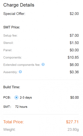
PCB cost
10 days from order to delivery here in London, UK, but I combined it with a much more complex 4-layer assembly order, so it may have been faster if this was ordered on its own.
While waiting for the boards to arrive, I designed a box for it in Fusion 360, and printed it on my trusty Prusa.
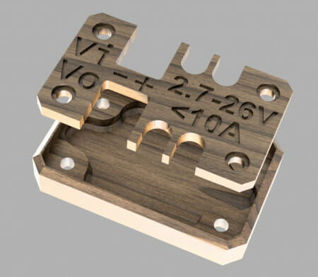
Render. Not actually wood, but wood looks more interesting rendered
And finally:
Assembled boards
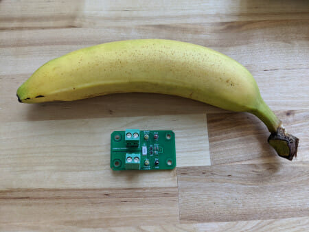
Connectors and test terminal posts soldered. Banana for scale.
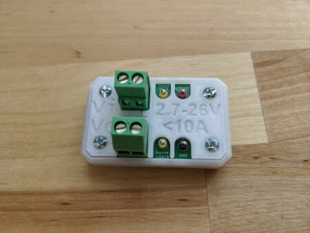
Put in the box
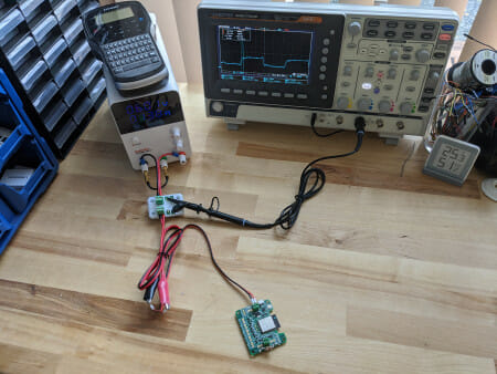
All wired up
Does It Work?
First, I set the scope channel to current mode at 1A/V (this is purely a display setting – the hardware doesn’t do anything differently in current mode), and the probe to 1X attenuation. 1X attenuation is not usually recommended because of the much lower bandwidth (10 MHz for my probes), but does give you lower noise. In this case it makes sense to use 1X because the amplifier only has about 100 kHz bandwidth anyways.
In current mode with the attenuation set correctly, all the measurements that used to be voltage are now given in current!
Channel settings
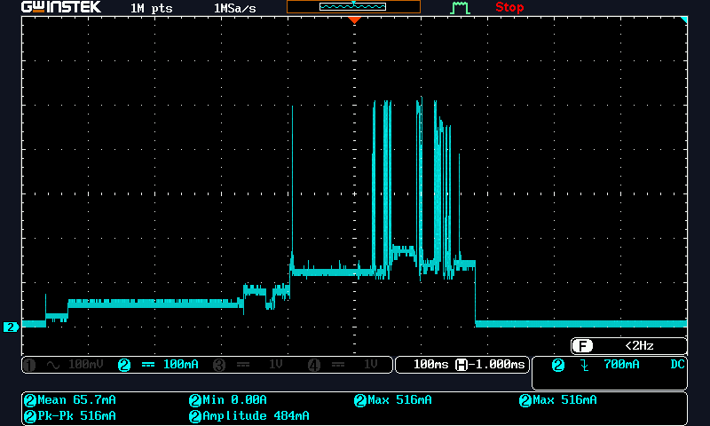
ESP32 Sleep. ~0mA deep sleep, 60mA wakeup for about 400ms during boot, then about 125mA during WiFi association, a few spikes to 500mA to transmit a few packets, then back to deep sleep.
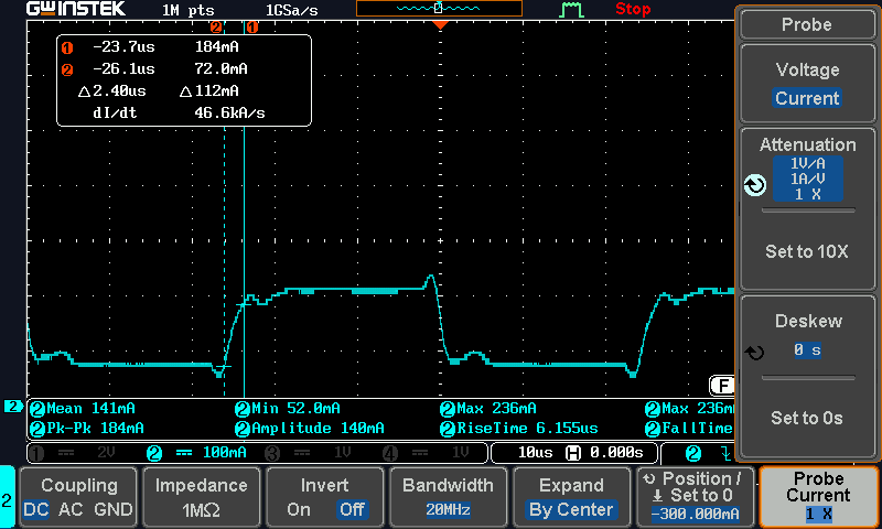
How much bandwidth do we have? For this test I have the ESP32 PWM a 44 ohms resistance (220//220//220…) at 20 kHz, with bulk decoupling capacitor removed.
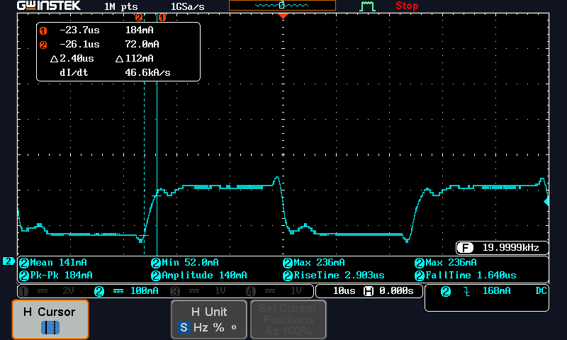
PWM.
Here we see a rise time of about 2.4 µs. That corresponds to a -3db bandwidth of about 145 kHz. Quite a bit higher than the advertised 80 kHz.
So it seems it does everything I want it to do, while being less than 1/10 the cost and 1/10 the size and clutter of a proper current probe.
What About Cost?
PCBs: $27.71
3D printer filament: 12.4g (~$0.48)
Test terminals: ~$1.00
Supply terminal blocks: ~$2.00
Total: $31.19 + various shipping. And you get 4 leftover partially assembled boards. If you assemble them and give/sell them to your friends and neighbours, that’s about $9 each.
These specs for this price? I am very happy. This is a good solution if you want current measurements faster than a multimeter, but not as fast as a proper current probe.
Files
All files below are hereby released under CC BY-SA 4.0.
KiCad: https://github.com/matthewlai/CurrentSense/tree/master/current_sense
Fusion 360 Case: https://a360.co/3fQznZr
Want Your Own?
Send JLC these files: Gerbers JLC BOM JLC Component Placement
Unfortunately I cannot provide any warranty or promise support. If you have questions, leave a comment below and I’ll try my best to help.
The only other components you need are the Phoenix terminals, 1.4mm test terminal posts, and access to a 3D printer if you want a case, as well as 4x 10mm M3 bolts, and 4x M3 nuts.