Using KiCad with JLCPCB Assembly Service
I wrote some tools to help with generating BOM and placement files for the JLCPCB assembly service from KiCad.
TLDR: Click here.
A Bit of History
I remember when I first started making PCBs in ~2010, our low spec (8 mil min traces / 8 mil min spacing) 2-layer boards costed $133 for 4 copies. Special academic pricing.
There were services like Sparkfun’s BatchPCB and OSH Park that were quite a bit cheaper, but generally took about a month to deliver, as they batched together designs from many customers on each panel to amortise the cost. Great if you are very patient, but not very useful if you have any deadline.
And then the Chinese prototyping services popped up, I think around 2012, and started getting popular. Of course, most production PCBs had been made in China for at least a decade at this point, but I believe this is the first time Chinese companies started targeting the low quantity prototyping market. If my memory serves, Seeedstudio was the first with their Fusion PCB service, and ITeadStudio was, as always, the first copycat. They offered about the same specs as the fabs we have been using, but for $10-$20 per 10 boards, though they still had the problem of long lead time (and high shipping cost from China if you want your boards fast).
Fast forward a few years to 2019, and now there are many similar services out there, offering even lower prices (as low as $2 for 10 boards!), very fast turnaround (24-72 hours), and very high specs (5/5 mils or even 3.5/3.5 mils). Very interesting options have also become available – ENIG finish, different substrates (eg. flex or aluminium for high power applications), different copper thicknesses, and 4+ layers for reasonable prices.
I have tried most of them at least once, and they are largely interchangeable unless you want very specific options. PCB prototyping is now a commodity, so now they are looking for other ways to differentiate, and assembly seems to be one such area. As hobbyists we have already given up making PCBs at home. Wouldn’t it be great if we can get someone to do the soldering as well?
I believe Seeedstudio was again one of the first to offer this service, but they assemble low quantity PCBs by hand, and reviews were scathing – bad solder joints, missed parts, parts installed in wrong orientation, etc. That’s why I never tried it. It didn’t seem like we would get high quality assembly until someone starts offering automatic pick-and-place for low quantity boards.
I was very excited when JLC started offering just that recently. They have a bunch of pick and place machines already set up with 600+ common components, and they can also load up new components for you at $3/component type, from their 30k+ components library. They are owned by the same company as LCSC, the biggest electronic component distributor in China, so that’s how they can get such an extensive library of components. Of course, with Chinese-sourced components there is always a chance of fakes. Time will tell how big of a problem that is – at least LCSC and JLC are very big companies that do have pretty good reputations they can lose, so it’s still not like ordering random components from eBay.
As far as I can tell their entire process is automated (besides presumably loading up reels that they charge $3/each for), and that also comes with downsides – no thru-hole components, and you can only use components they have in stock (unlike most assembly services, you can’t supply components for them to use). Unfortunately they don’t have any connectors in their library, so if you want a USB connector for example, you still have to solder that yourself. The reason they gave is that they panelise boards for assembly, and board-edge connectors make it difficult. However, besides that, their library is pretty extensive, with even some stock of high end microcontrollers like STM32F7, and lots of STM32F4.
The Process
I have developed a process for using their service with KiCad, and wrote a script to generate the files they need, so here is a walkthrough.
- Design your board as usual, but…
- Make sure all the SMT parts you want assembled are on the same side.
- Choose parts from their library. Add the Cxxxxx code to your components in Eeschema by adding a custom field (call it anything you want). That’s what my script will pick up later on. Anything that doesn’t have a Cxxxx code won’t be assembled.
- Once you are satisfied with your board design, go to Eeschema and run “Tools -> Generate Bill of Materials” to generate a BOM in any format/plugin. We don’t actually need the generated BOM file, but this process will produce an intermediate netlist file in XML format that we need later (not the same as KiCad’s standard netlist).
- Go to Pcbnew and run ‘File -> Fabrication Outputs -> Footprint Position (.pos) File’.
- CSV format, mm unit, and ‘single file for board’
- Plot gerbers as per usual for PCB manufacturing – all copper layers, front mask, back mask, front silk, back silk, Edge.Cuts (for board border). Not sure if the paste layers are needed (given they are doing the assembly), but I include them in my zip file anyways and they don’t seem to mind.
- Run my script and give it the project directory. It will look for the files it needs in the given project directory and all sub-directories, and let you know if it can’t find anything.
- Follow the instructions here to install and run the script: https://github.com/matthewlai/JLCKicadTools
- If all goes well, the script will tell you where the BOM and CPL files generated are (inside your project directory). If not, read the error message and fix anything that needs fixing.
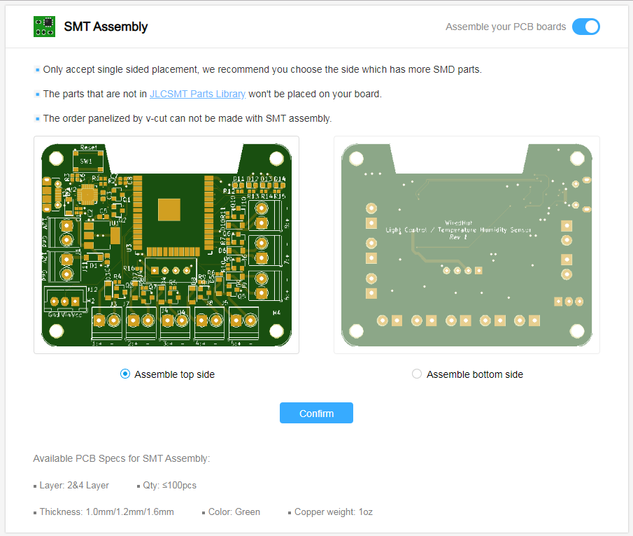
- Go to the order page and upload gerbers and pick options as usual. Keep in mind that only green soldermask and 1oz copper is supported for assembly. In ‘SMT Assembly’, click the button to enable assembly. Pick a side to assemble, and confirm.
- Upload the files generated by the script. Next.
- You’ll get a list of matched parts found. Check each one, and click “confirm”. You have to confirm every part before you can proceed.
- Very important: Zoom in on the mockup diagram, and make sure all the polarities and orientations as indicated are correct. Some of them probably won’t be, because KiCad footprints seem to have different canonical orientations.
- Note down the footprints with incorrect rotations, and the additional rotation required to make them correct (positive is clockwise).
- Edit ‘cpl_totations_db.csv’ in the same directory as the conversion script to add those footprints. The first column is the footprint pattern to match in regex, and the second column is rotation correction.
- Run the script again to generate new BOM and CPL files. Go back on the JLC page and upload those new files. Repeat until all orientations are correct, and place the order! Keep in mind that unless you are using very expensive components, the price for 10 boards will be very similar to the price for 5 boards (minimum quantity) because most of the cost is in setup. I would order 10 if there’s any chance that you’ll need more than 5.
- Please contribute your corrections to the db file so others can benefit. Either do a GitHub pull request if you know how, or just send me a quick message at [email protected]. Thanks!
- Wait for the board to turn up and solder all your thru-hole and other additional components.
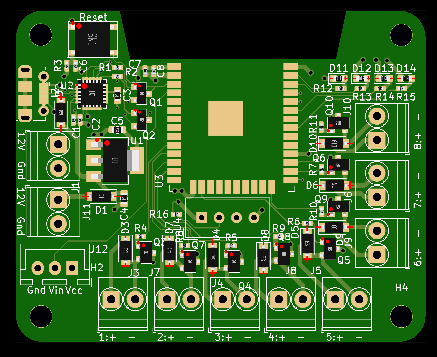
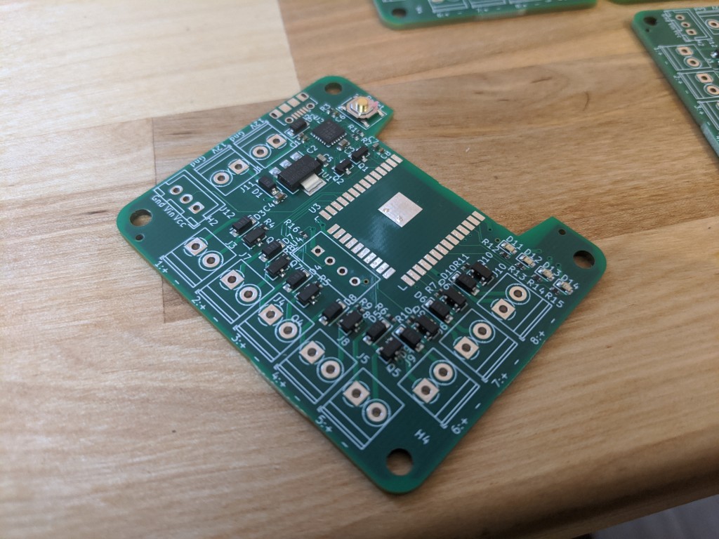
The board I’ve decided to test this on is a ESP32-based WiFi 8 channel PWM controller with a USB-UART adapter IC (Silicon Labs CP2104) and a few auxiliary sensor inputs. On a 6x5cm 4-layer board (mostly screw terminals). I probably could have made it 2-layer if I really wanted, but given how cheap JLC’s 4 layer boards are, I decided to use it as an exercise to see how small I can make the board, with nice power and ground planes. I used a QFN USB interface chip (I probably wouldn’t have if I was soldering this by hand) and plenty of 0402 passives. There are about 50 assembled parts in total per board. The only parts they couldn’t assemble are the ESP32 module, and all the connectors. They should all be pretty easy to hand solder and I am happy that I don’t need to order and organise storage for all those different jellybean components.
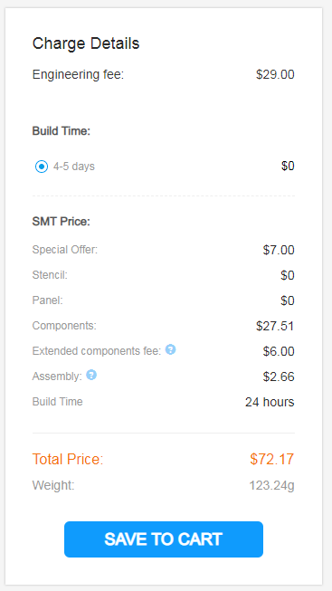
The whole thing came to $72.17 before shipping. Including 10x 4 layer boards, $27.51 worth of ~500 components (total for 10 boards), and assembly. How amazing is that?
A bare 4 layer board would have costed more than that just a few years ago.
If I really optimised it for cost by squeezing it into 2 layers and soldering it myself, I probably could have gotten it for maybe $30 less. But it would have taken a few more hours of my time at the very least. Is that a worthwhile trade-off? For me, trading $30 for a few hours of my time is a no-brainer.
If you are a hobbyist who still gets pleasure from soldering, maybe the service isn’t useful to you, but I’ve soldered enough TQFP FPGAs by hand in my life that I’m very happy to let someone else do the soldering, so I can focus on more interesting bits. Especially when that someone else is a machine that can solder much better than I can by hand.
Results
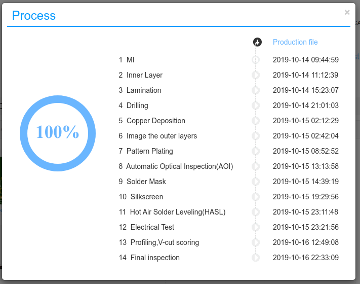
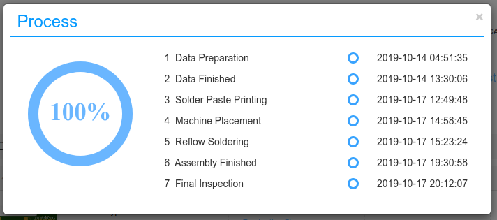
8 days from order to delivery to London, UK, using their DHL shipping option ($19.36). This is a 4 layer board, and they say 2 layer boards should be a few days faster. They also have a nifty progress checker on their orders page.
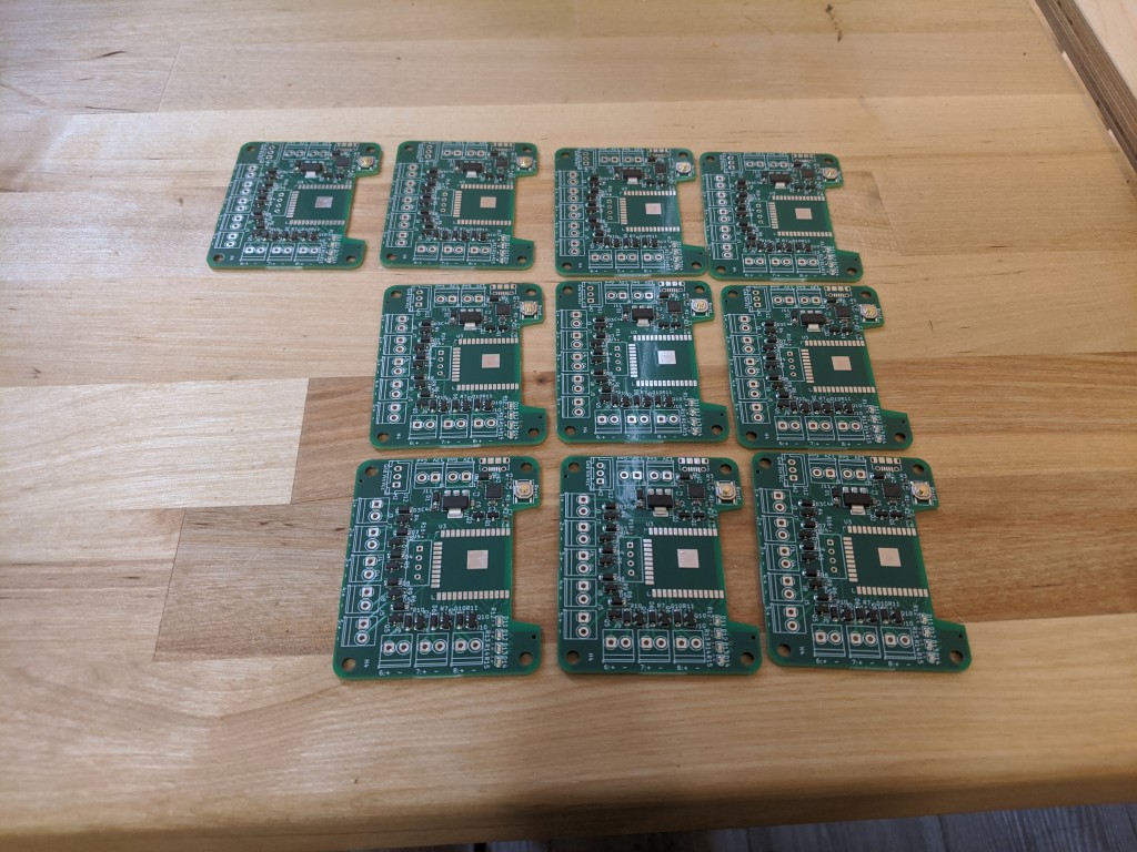
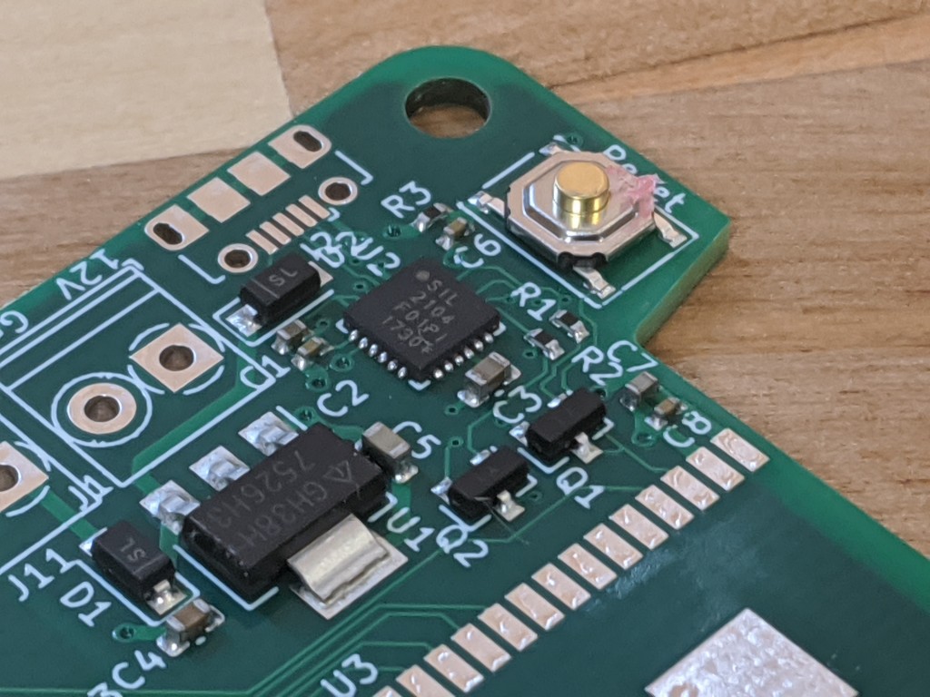
Quality-wise, there’s really nothing I can nitpick. It’s perfect. The QFN and all the 0402s all look amazing, and no reflow solder residue (tiny solder balls) anywhere. There is some extra solder on the ESP32’s unsoldered pads, but that’s typical of HASL process, and those pads were not reflowed. It also looks much worse in the picture than in real life. They are pretty flat in real life, but of course if you are doing BGA you should opt for ENIG finish for better co-planarity (they offer that for about $20 extra).
I am totally blown away and will be using this service a lot more in the future. No more soldering millions of simple components!
Happy making!
Notes:
- Conversion script: https://github.com/matthewlai/JLCKicadTools
- My test board: https://github.com/matthewlai/WiredHut/tree/master/hardware/light_control/light_control
