We built a web-connected LED matrix driver for a team of about 500 people, over 4 months. This post is about the hardware design.
At the end of last year Fede Heinz, a colleague of mine at Google reached out for a collaboration on his Blinkenlights project, to build a web-connected LED matrix driver for his team of about 500 people. It took about 4 months, but the hardware design part of the project has finally come to an end, and in this post I will talk about the hardware design, and how we made all the important design decisions, as well as all the problems we ran into (some of them pretty funny in hindsight). The goal is to give everyone an LED matrix with the controller board, so they can send 16×16 images to each other. We went through quite a few brainstorming rounds and design iterations, but in the end decided to build an ESP32-based driver board, powered by a computer through USB-C, and drives an external matrix. This project is open source hardware and software, and you can find the hardware design on my GitHub repo, and the firmware/software on Fede’s.
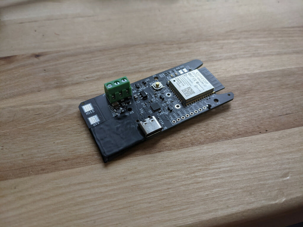
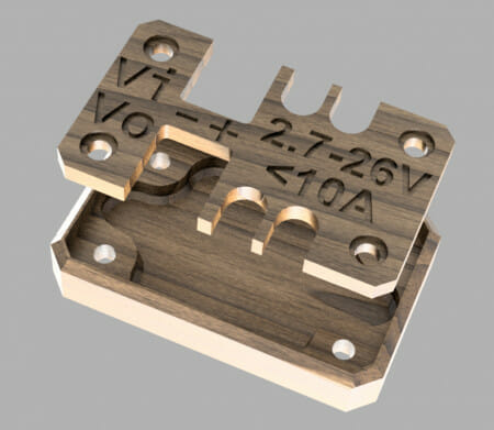
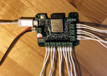
BlinkenLights!
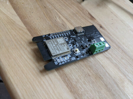
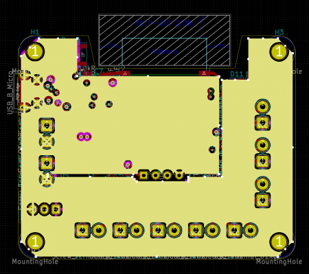
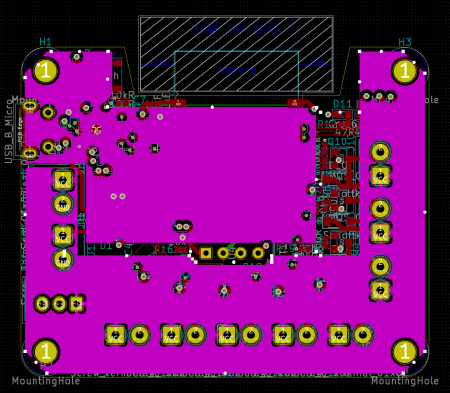
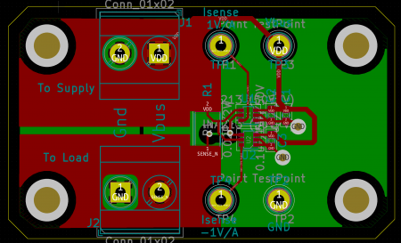
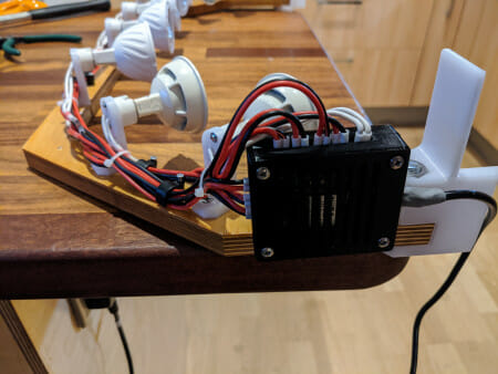
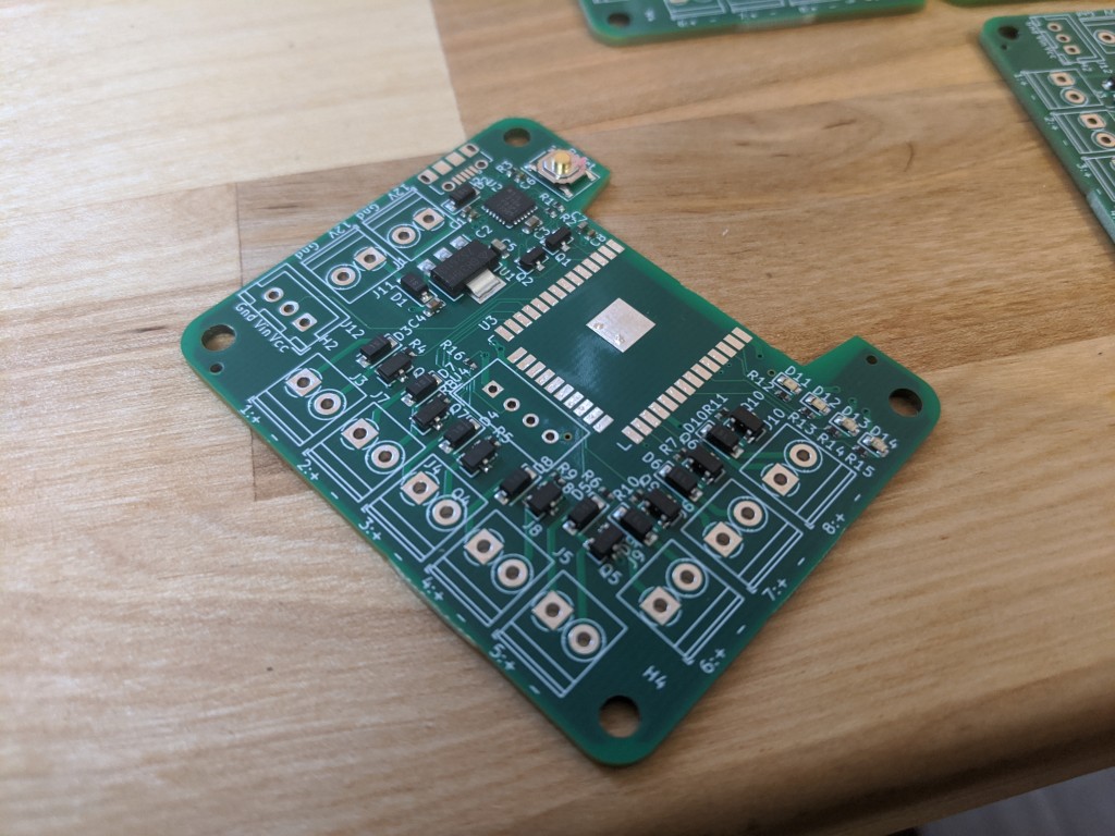
Blinkenlights PCB
The PCBs for this project were manufactured and assembled by JLCPCB.
High Level Design
Internal vs external matrix
Once we decided on making a custom PCB, we thought it would be cool to have the matrix built-in to the board. JLCPCB has the WS2812 in their catalogue, and it would only be slightly more expensive than buying the matrices separately. Our first prototype included the matrix. Unfortunately the defect rate was unacceptably high – we had 256 LEDs per board, and a defect rate of about 1% of the LEDs, which means we had no totally working boards!
We don’t really have the equipment (an x-ray machine) to figure out why, but as the WS2812 is extremely moisture sensitive at MSL (moisture sensitivity level) 5a, that’s our best guess. This has caused problems for a lot of people. If we were going for higher quantity it may have made sense to work with the assembly house a bit to try to solve this, but at 500 it doesn’t really make sense, so we decided to use an external matrix instead. We talked to them about this and they took it off their parts library to investigate, but couldn’t guarantee anything.
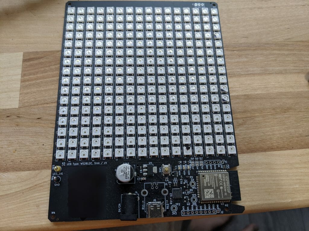
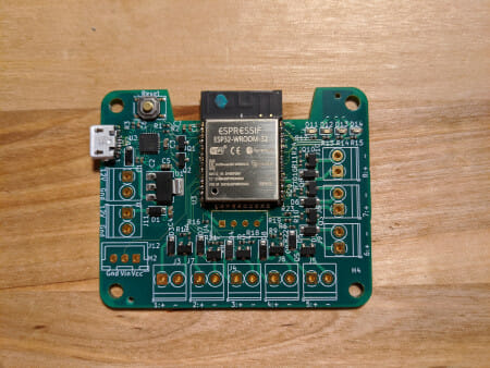
Rev 1 – with integrated matrix
USB-C Data + Power
We need the board to connect to a laptop for data, and the original plan was to include a USB-C connector for that, but have a separate barrel jack for power (you can see this setup in the Rev 1 board above).
But we had a pleasant surprise – as it turned out, all modern laptops with Type C ports can actually supply 1.5A or 3A, and since that’s enough for our use case, we get to save the cost and logistics trouble of providing a separate power supply, all while helping to reduce e-waste.
Note: taking that much power from USB-C ports safely and in a standard-compliant way requires care. I have written a post on that topic. Please do not just draw that current without checking.
We are also only supporting laptops with native Type C ports, using C-C cables. This makes our life easier because we don’t need to support the whole pre-C mess with the Battery Charging Specification. We can do this because we are only distributing these boards within Google, so we know (almost) everyone has a recent laptop with Type-C ports. If this was going to be more widely distributed, it would probably be a good idea to support BCS, and maybe with another Type-C port that can use a Type-C supply for power.
Microcontroller Choice
We wanted something a bit more beefy than an AVR, but we also want Arduino compatibility because we will be encouraging users (who are mostly programmers but not electronics engineers or firmware engineers) to hack it, and being Arduino-compatible makes it much easier.
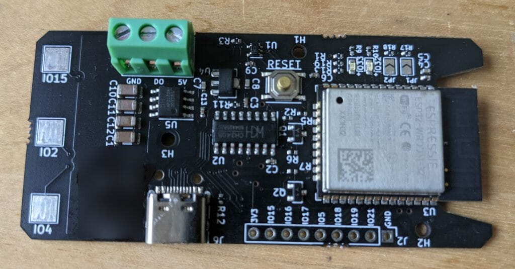
The ESP32 is an obvious choice – it’s cheap, fast, and has good Arduino support. We don’t actually have plans for WiFi or Bluetooth, and it was still the most cost effective option regardless. Our boards end up costing just over US$4 each manufactured and assembled, so the cost of the ESP32-WROOM-32 module is actually responsible for just under half of the entire cost of the board ($2.0061 from JLCPCB, at 500 qty).
Would be cool to have a microcontroller with built-in USB support so we don’t need a separate chip, but all the ones with built-in USB I have used cost much more than $2, so would not be cost-effective even taking into account the elimination of the USB-UART chip.
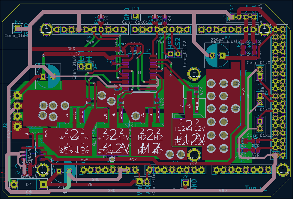
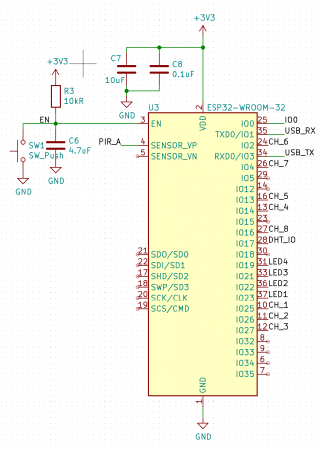
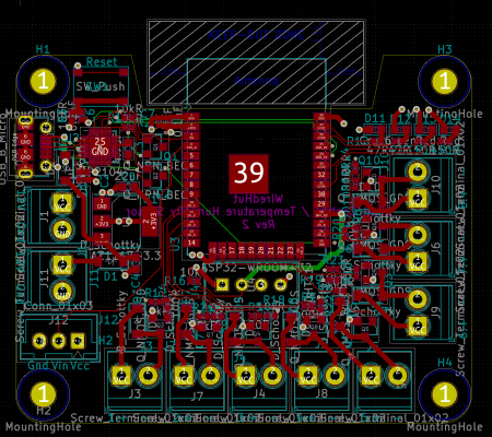
Schematics
Full schematics: PDF
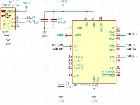
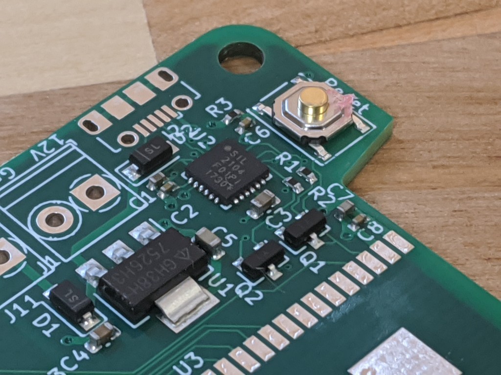
The schematics design is pretty straight forward on the microcontroller side, with the ESP32 module, a CH340B USB-Serial adapter, the standard 2-BJT reset circuit to allow automatic reset from Arduino (more accurately esptool). The reset circuit has slightly different capacitance value from the official recommendations from Espressif, because I found that with the official values it doesn’t reset reliably on Windows sometimes.
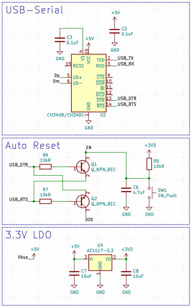
Power, USB-serial, auto-reset
See this post for more information on the USB-C part.
I am not a big fan of the CH340 series because the documentation is very sparse, and it doesn’t have a SUSPEND output, which is realistically required to support USB suspend. However, it is available in SOIC package, whereas my preferred chip, the CP2102, is only available in QFN. We used the CP2102 in our first revision prototype, but found that we had a soldering defect rate of about 10%, which is approximately what I have found with my past projects using the same chip. It’s fine for a personal project where I can fix them manually when needed, but we don’t want to have to fix 50 boards in a 500 boards run! If we were building more, it may make sense to try to tweak the footprint a bit to see if we can improve assembly defect rate, but we didn’t want to delay this project. So we switched to the CH340B instead. Those chips are in every low cost ESP32 board and USB-Serial adapters these days.
I quite like the AZ1117 family of regulators for ESP32, because they are rated for 1A, and come in tiny packages (SOT-89 in this case). Here is a nice comparison of standard SMT package sizes. At this package size it can’t handle 1A continuously, but we only need the 1A for current spikes. ESP32 requires up to about 800mA with WiFi and Bluetooth on, but those are always very short spikes, and on average usually it only needs about 100mA. A 1A regulator in a small package is perfect for this kind of applications.
The other significant part is the LED matrix interface:
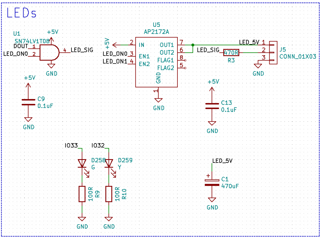
LED interface
Here we need a level shifter, because the WS2812B uses 5V signalling, and the ESP32 has 3.3V IO. But in addition to that, we also need to power-gate the matrix because it draws about 250mA idle, which exceeds the 100mA maximum we can legally draw from USB without negotiation (and without CC current advertisement / BCS detection). So we have an AP2172A chip that we use to switch on power to the LED once we know we can draw that current.
The AP2172A actually serves another very important purpose – we need a large capacitance on the LED side for voltage stability, but USB only allows a maximum of 10uF on Vbus. If we connect a 470uF capacitor to Vbus directly, there is a good chance that the host will go into an over-current reset while the capacitor is charging up. We did in fact see this in an earlier prototype without that chip.
With the AP2172A, it will limit the charging current to 1.5A per channel (it has 2 channels that we wire up in parallel), so we can have any amount of capacitance on the LED side. We control the chip using the LED_ON0 and LED_ON1 signals. Why two signals? Because we can get either 1.5A or 3.0A available from the host, and if we only have 1.5A available, we can’t charge at 3.0A. Once we have the capacitors charged, we always turn on both channels to reduce the channel resistance, and apply current limit in firmware instead.
The level shifter is a TI SN74LV1T08, with an AND gate built-in. Why AND gate? Because most chips really don’t like an input voltage higher than supply voltage. This can lead to the input pin powering the whole chip through the ESD protection diodes (which wouldn’t have been rated for this), or latch-up. With the signal ANDed with LED_ON0, we ensure that the data pin can never be driven high when the LED power is not on. I like to apply this kind of protections in hardware in addition to firmware just in case, especially since we will be encouraging users to experiment with the firmware.
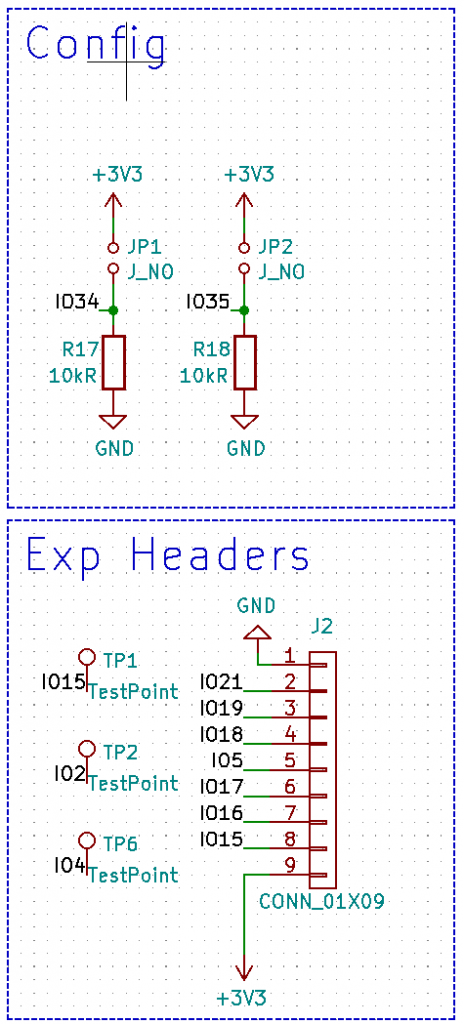
And then we have config strap pins. They are basically input pins connected to a pull-down, with an open solder jumper to Vcc. This allows the user to set some semi-permanent config options that we can support in firmware. They are like DIP switches, but free and take up less board space! (though slightly harder to use)
We also have the extra pins we aren’t using exposed on a header, as well as 3 capacitive touch buttons (for user experimentation). Remember to always put ground and Vcc on expansion headers!
Straps and expansion headers
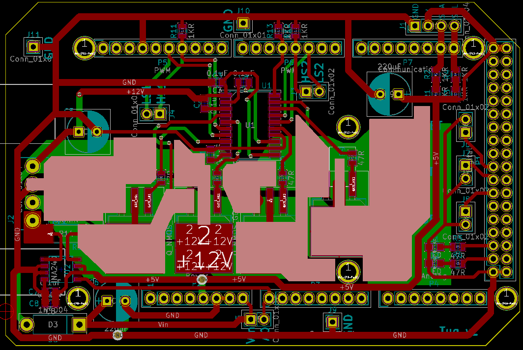
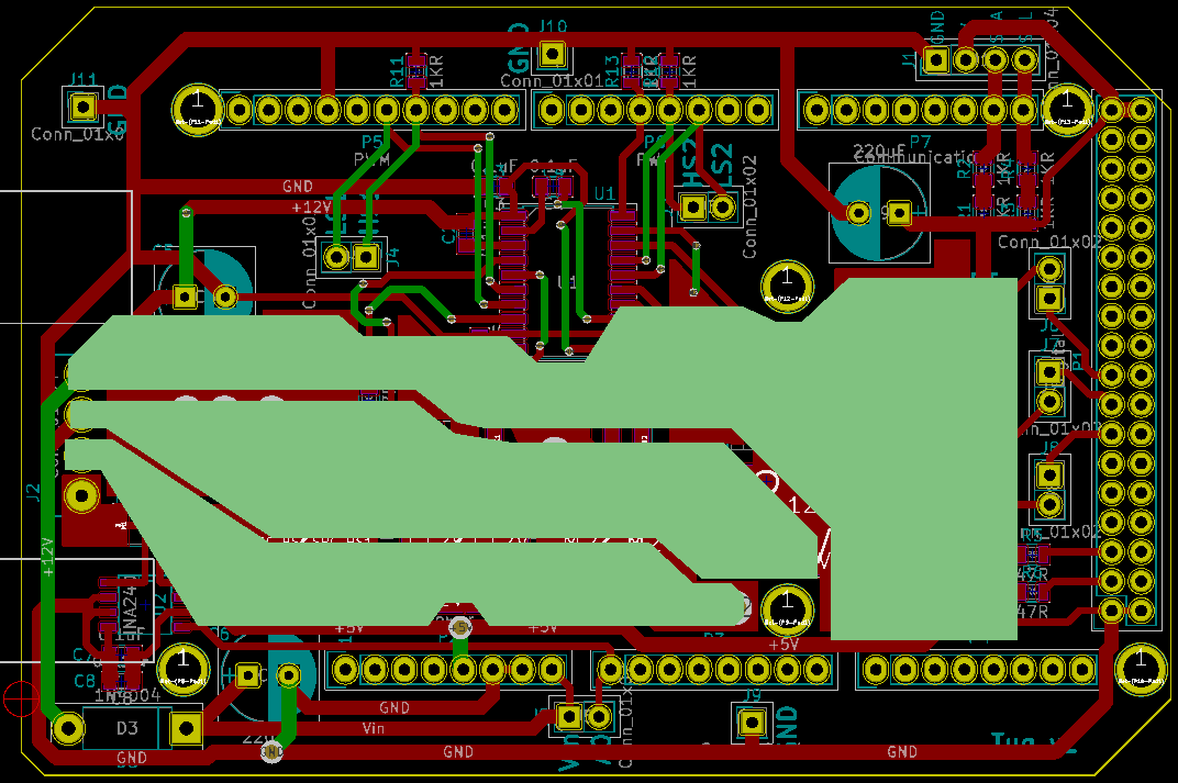
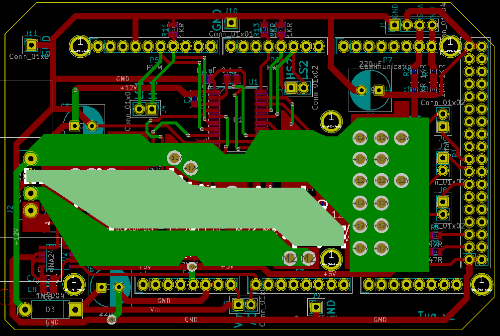
PCB Design
We decided to go for a 2 layers design in this case, because it’s slightly cheaper. At 500 qty we would be paying $0.21/ea for 2 layers, and $0.38/ea for 4 layers. It’s not a lot, and that’s why I have not designed a 2 layer board for my personal projects in a very long time, but for 500 boards it does add up, and 4 layer boards would also restrict us to green soldermask with JLC assembly service. This is a relatively simple board, and easily doable on 2 layers, so we went with that. It does mean we cannot have impedance-controlled traces for USB, but since we are only going for Full Speed, it’s not an issue. At 20ns minimum edge rate for Full Speed, transmission line effects only become significant at ~60cm.
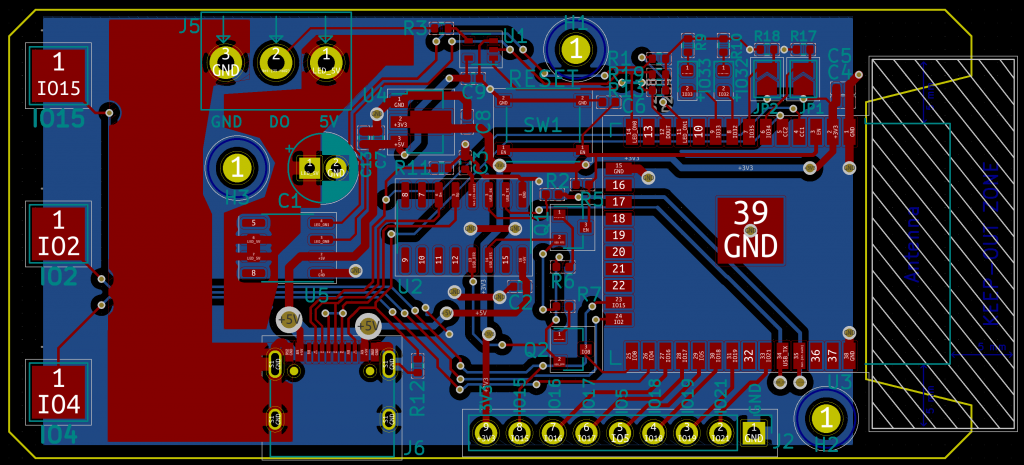
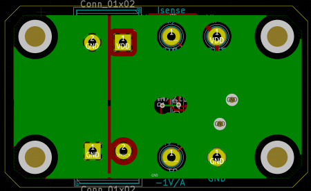
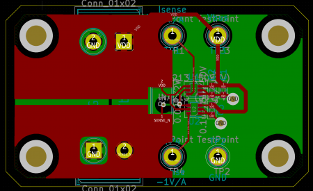
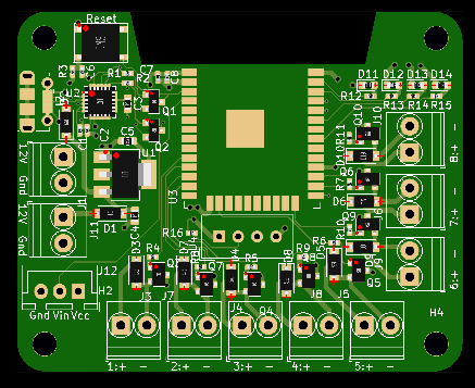
PCB layout
We have a rectangular layout with the LED connector in a screw terminal on top, USB-C connector on the bottom, and the ESP32 antenna on the right with a cut-out. The capacitive touch buttons are on the left side to allow them to be exposed if we have a case covering up the rest of the circuit.
U2 is the CH340B that takes up a lot of space due to the huge SOIC footprint. The CP2102 would be much smaller, but that doesn’t help if we can’t get it soldered reliably!
We are using an aluminium solid polymer capacitor for bulk decoupling of the LED matrix. It’s about $0.03c more than a standard aluminium wet electrolytic capacitor, but it’s smaller and higher performance (probably doesn’t actually matter for this application). We actually used ceramic (MLCC) capacitors in an earlier prototype to keep the board height lower (see picture at the beginning of the post), but unfortunately ran into acoustic noise issues at high power settings due to the MLCC dielectric being piezoelectric. The other option to keep the board profile low is with a tantalum capacitor, but I avoid using them when possible because tantalum is a conflict resource. A few manufacturers say their tantalum is conflict-free, but I’ve never really looked into that, and have never really needed to use tantalum. Tantalum is also much more expensive, and have a very exciting failure mode (with an explosion). Be very careful with those!
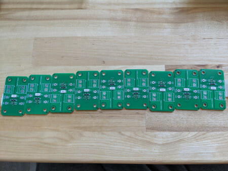
Panelisation for Manufacturing
PCB fabs generally don’t want to deal with hundreds of tiny PCBs, and would rather deal with fewer larger ones instead. For example, JLCPCB has a limit of 50 PCBs for assembly, so since we want more than that, we need to put our PCBs in larger grids called panels. This is what our panel looks like:
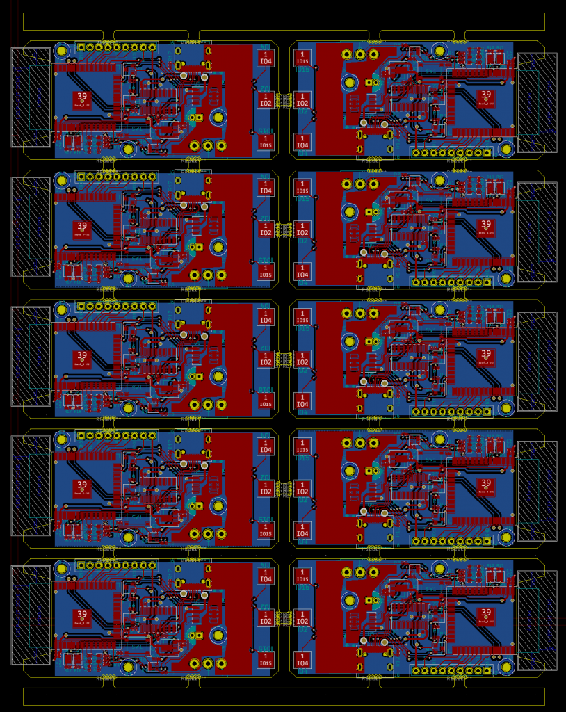
5×2 PCB panel
Different fabs have different preferred panelisation techniques, and JLC requires tabs and mousebites for assembly, which is what we have here. The boards are connected by those little tabs lined with drilled holes, so they can be manufactured and assembled as panels, and we can just break them apart by hand once we receive them. There are rails on the top and bottom – they give the panel some extra rigidity during assembly, and also serve as a place to put order numbers, fiducial marks (marks on the PCB for pick-and-place camera calibration), tooling holes, etc. Those are usually added by the PCB fab, and not something engineers need to care about. Just leave some room for them to do their job. JLC’s panelisation specs and recommendations are here. My panels were generated using yaqwsx’s KiKit tool, and you can see my config here. It has been successfully manufactured by JLC and seems to work well.
Cost
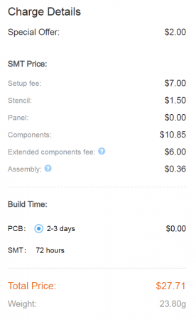
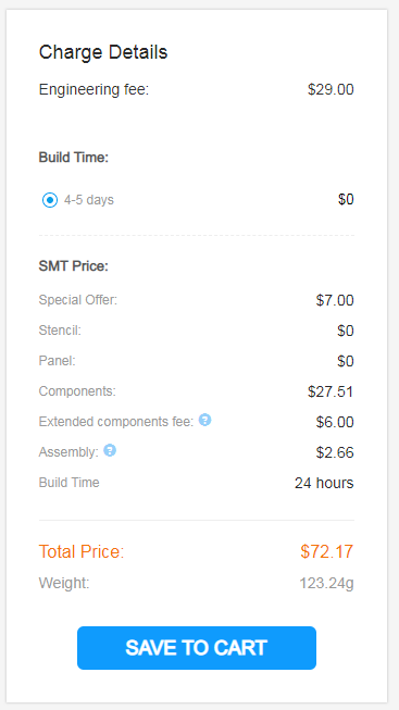
Altogether, the cost is $140 for a 2 panels assembled prototype (20 boards, $7/board).
That comes down to $462 for 10 panels (100 boards, $4.62/board), and finally $2103 for 50 panels (500 boards, $4.20/board).
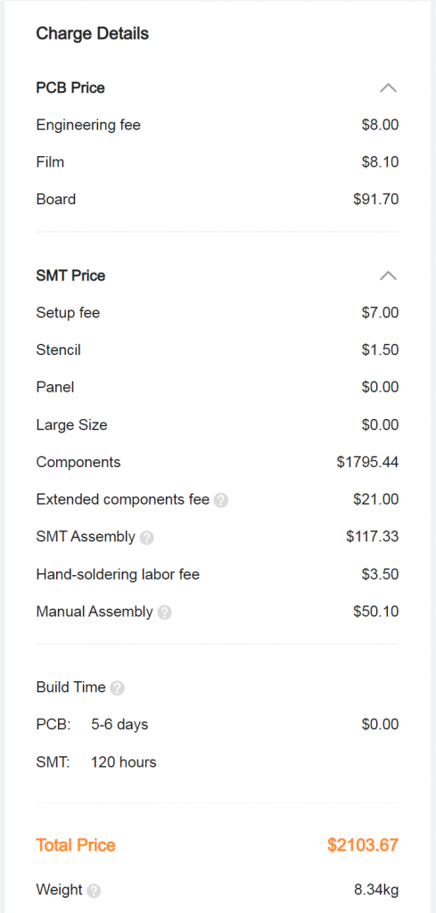
Cost breakdown
Most of that is ~$1800 for components. That’s about $3.60 component cost for each PCB, most of which is the ESP32 module at $2, the CH340B USB serial chip at $0.60, and the AP2172 USB power switch at $0.35. It’s amazing that everything else (regulator, a bunch of capacitors/resistors, some transistors, a level shifter, and a few LEDs) only add up to $0.65.
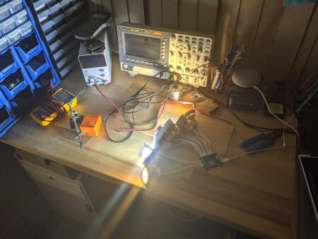
Testing
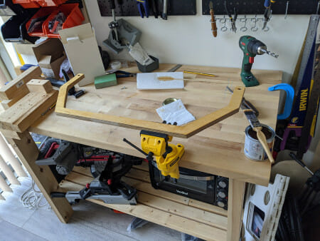
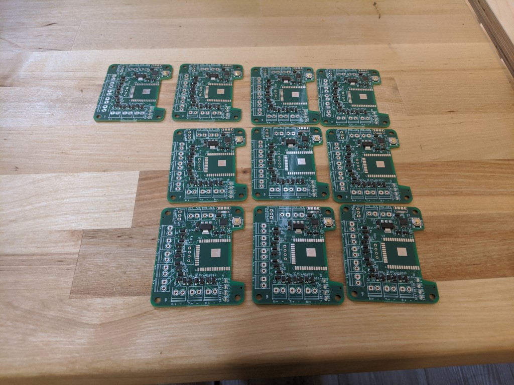
A few days later, our prototype panel arrived! (this is the version with MLCC capacitors that like to sing)
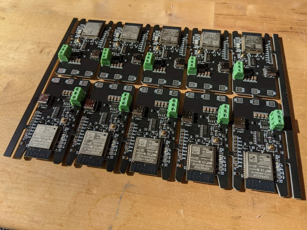
Prototype panel
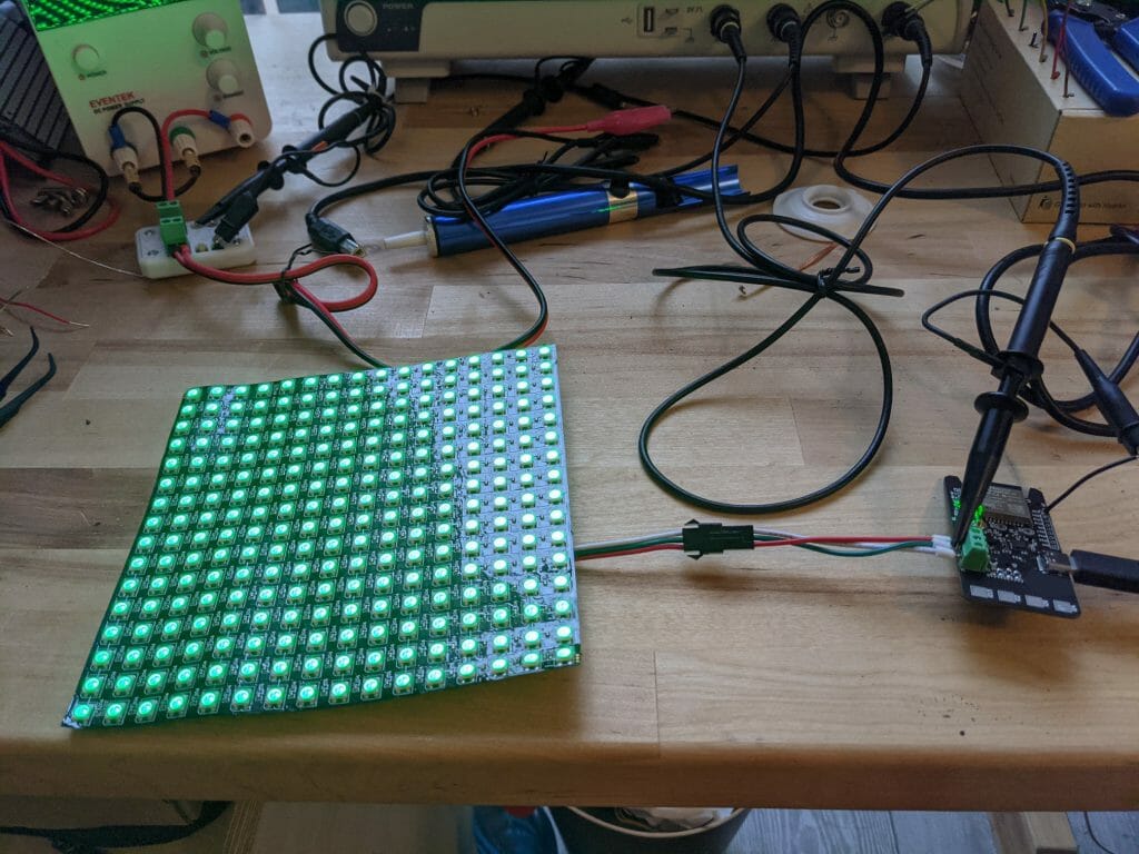
The panel breaks up easily by hand and pliers, so it’s time to do some testing.
Functionally they all flashed fine, which is encouraging (we had problems due to CP2102 soldering defects before). After verifying that all the boards work with my laptop, it’s time to break out the scope.
I don’t usually do such extensive testing on my personal projects, but since this is going to a lot of people, it’s important that we are well within spec since something that is marginal may just happen to work on my laptop, but not others’, and we can’t realistically test it on everyone’s laptops. USB is the interface between our users’ laptops (which we can’t control), and our boards (which we can), so that’s the focus of our testing. We really want to be standard-compliant here, because that means if the laptops are also standard-compliant (and they should be), we will have a working combination.
Also, I am of the opinion that if we put a USB port on our board, we should make sure it’s compliant. I’m less strict about it if it’s just a prototype and I’ll be the only person using it, but if we are selling or giving away devices to others, I try very hard to stick to the spec.
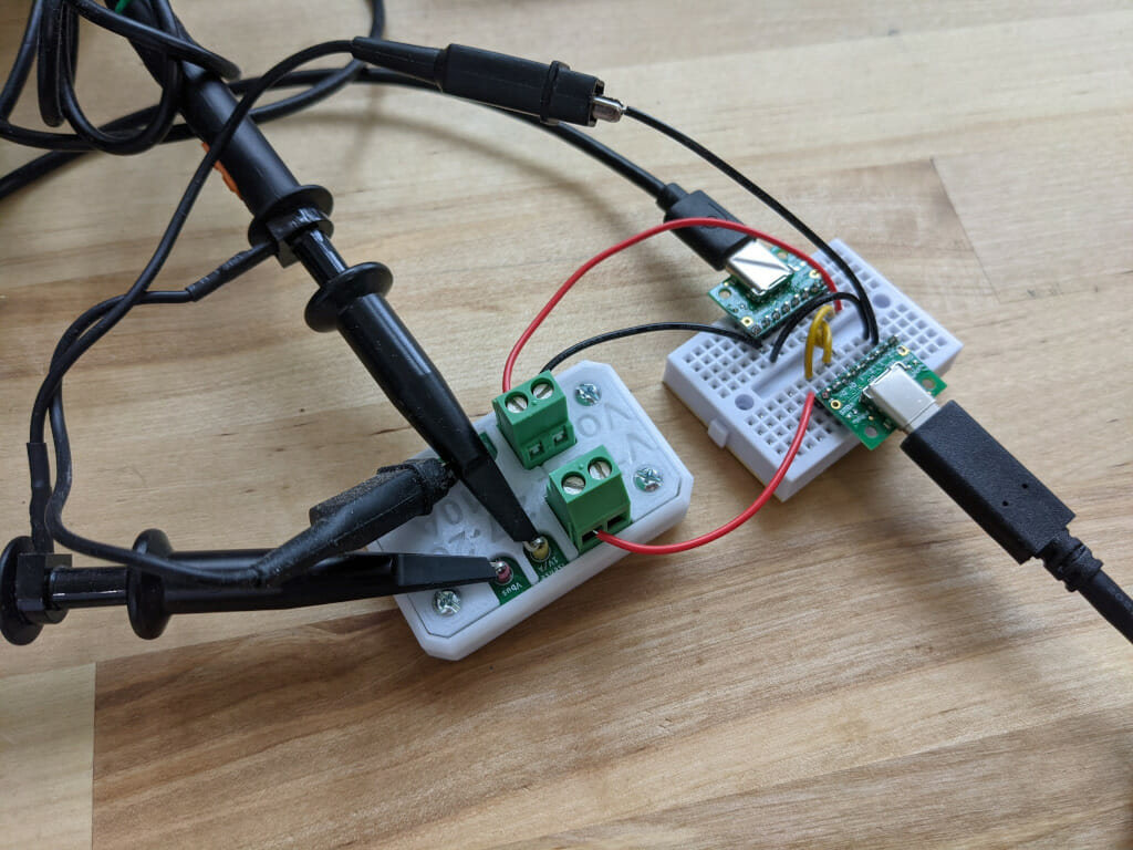
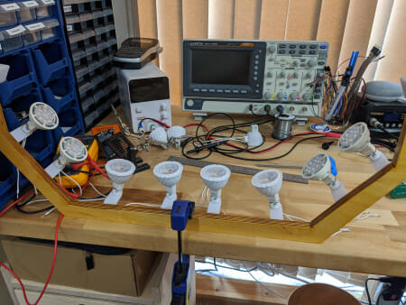
This is the USB-C probing setup using two USB-C breakout boards (with the pulldown resistors removed), and my cheap DIY current probe board.
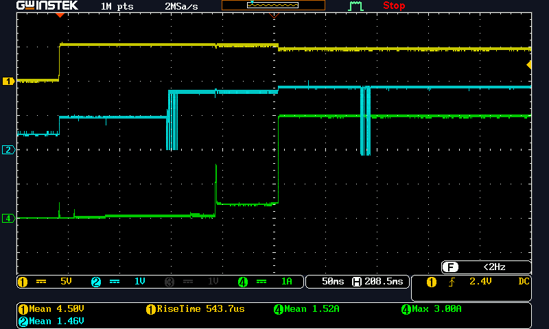
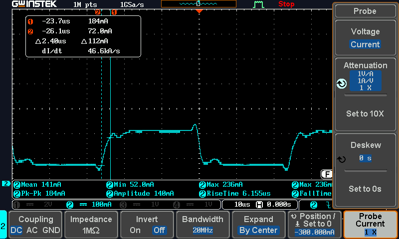
Some cool scope shots, with the board plugged into my MacBook Pro. First we have the plug-in
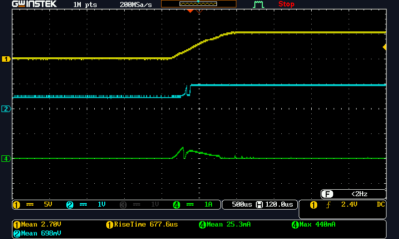
Yellow: Vbus, Blue: CC, Green: Ibus
We see that we draw up to 500mA in the first 50 microseconds or so to charge the regulator input capacitance, but at Vbus = ~1V, the regulator turns on and the second pulse starts to charge the capacitances after the regulator, with a nice ramp up and down. We are down to almost 0 current at approximately 200us, once all the capacitances have been charged.
We also see that CC is ~1V, which means the MacBook is advertising 1.5A available.
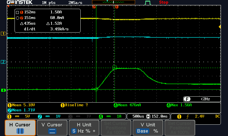
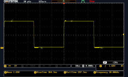
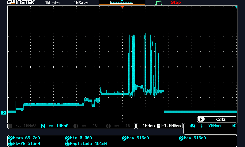
Then we zoom out a bit to see the entire sequence to power-on of the LEDs.
Yellow: Vbus, Blue: CC, Green: Ibus
We see that as the ESP32 boots up (around -3.5div, which is about 50ms after plug-in), current draw increases but is still much lower than the 100mA limit. At -2div, the MacBook changes current advertisement to 3A, and simultaneously sends a Power Delivery message. If we have a more sophisticated controller we can try to decode that message and negotiate using PD instead of the much more crude CC current advertisement mechanism, but we don’t, so we ignore it and just wait for it to stabilise (this is allowed by the standard – devices that don’t understand PD must wait a minimum of 10ms after CC voltage changes to make sure they are not confused by PD messages). Finally, at about -1.2div, our firmware confirms the 3A available change, and turns on the USB power switch to charge the big capacitor, which is the current spike at -1.2div. Once the capacitor is charged, we get back down to about 300mA idle current for the LED matrix. Finally, at +0.1div, we turn the matrix on to all white for testing, drawing 3A. This part looks all good, so let’s zoom in to that capacitor charging spike.
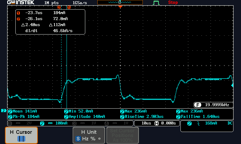
Yellow: Vbus, Blue: CC, Green: Ibus
Here we see that we are not exceeding the 1.5A current limit (we designed the firmware to always charge at 1.5A, even though we actually have 3A available in this case). We see that the AP2172A chip is doing its job with a ~500us soft start, and then limiting the charge current to 1.5A, giving us the plateau waveform.
Note that the soft start limits our current slew rate to 3.49kA/s (between the 2 cursor points on the screen). USB spec actually has something to say about that as well – there is a limit of 150mA/us (150kA/s) on current slew rate, so if we limit our current draw to 1.5A, but jump right up to that faster than 150kA/s, we would still not be complaint. Using a USB power switch makes complying with this part of the spec much easier.
Now let’s look at when the LEDs are suddenly turned on to max power (this is the worst case).
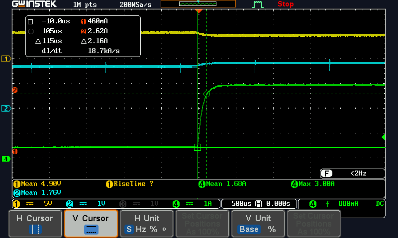
Yellow: Vbus, Blue: CC, Green: Ibus
We see that the current is limited to 3A (we have a safety margin in our actual firmware – I removed it for testing), and the current slew rate is at 18.7kA/s. If the current slew rate is too high here, we could have compensated for it by increasing the size of the big capacitor, but we are well within the limit here.
Everything looks good on the USB side! I didn’t try to verify actual USB data because that’s handled by the CH340B chip, and I assume it’s compliant since it’s used in many commercial products, and there’s really nothing we can do if it isn’t.
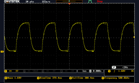
The next thing to look at is the LED data stream. First a zoomed in view of the pulse shape.

LED data pulses
The voltage levels look fine, and the edges also look fine. They are a bit overdamped with the 470 ohms series resistor, and that’s why the edges are a bit rounded. But 88.6ns fall and 61.6ns rise is still plenty fast enough for this signal speed, and much better than being under-damped, since ringing can read as additional edges. This also allows the user to use longer wires, where the higher inductance would require more damping.
Some pulse statistics when zoomed out:
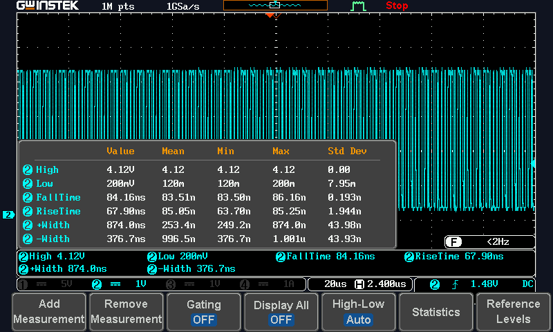
Signal statistics
Here we see that the short pulses are 250ns, long pulses 874ns, which are well within spec (220ns – 380ns, and 580ns – 1000ns respectively).
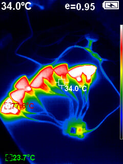
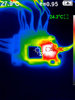
This concludes the scope tests, and just for fun, I also took a picture with my IR camera. This is useful to spot if anything is getting unexpectedly hot.
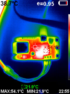
IR image
The 3.3V regulator and the USB power switches get hot, and that’s as expected. The USB power switch only gets up to 54C, which is acceptable. The chip is fine at this temperature, and 54C is actually also lower than the 60C maximum recommended temperature for exposed heated surfaces in ASTM C1055 (“Standard Guide for Heated System Surface Conditions that Produce Contact Burn Injuries”), so in terms of contact burn risk, this is safe as a consumer product even without an enclosure to stop the user poking the hot bits… at least if the ambient temperature is no higher than about 28C, which would put the chip at 60C.
This concludes our testing! We will be doing the mini-production run soon.
Lessons Learned
This is my first ever project to be produced at this kind of quantity, and it has been very interesting experience learning about all the different considerations that go into designing for manufacturability (and design for availability, given the current chip shortage). It’s not difficult, but there are just so many things to think about even for a relatively simple design like this. First we had soldering defects that I would normally not worry about too much but is unacceptable to fix manually at quantity, then we had random basic chips going out of stock between each prototype iteration, chips failing (probably) due to moisture handling, capacitors becoming piezoelectric buzzers, and then there’s the much more extensive testing required to gain confidence that the design will work with a wide range of hardware that we cannot exhaustively test. All very different from personal hobbyist projects where I only need to make sure they work for me, and can do a lot more trial and error, as well as manual hacking to fix things. I knew all those things in theory before, but it’s very different putting them all into practice.
And then of course there is a whole another level out there, designing products that will be produced in the thousands or millions, and require going through certification. As a hobbyist engineer, I will probably never get to work on a product like that, but hopefully I’ll get to do another >100pc design at some point!
I am also in awe how (relatively) easy and affordable getting our boards made and assembled is. With JLC’s assembly service they supply all the parts from LCSC, so although it does mean you have to design using the parts they have, they do have a pretty extensive library, and if your design works with just their components, it’s about as turnkey as assembly services get. You don’t have to worry about sourcing and shipping parts to them, or have them source your parts and potentially end up with “substitutes” that don’t actually work in your design, or counterfeit parts, as you would with other assembly services. To be fair, we did run into some assembly quality problems that required designing around (the LEDs and the CP2102 chip), but still, I’ve always imagined getting boards assembled would be much more work than this as a hobbyist.
Disclosure: JLC sponsored some of my projects.
]]>


 build-up, which I have since decided to filter out.](/images/wp-content/uploads/2020/08/IMG_20200327_164146-2-450x340.jpg)


. Or maybe you have an air leak somewhere?](/images/wp-content/uploads/2020/07/IMG_20200715_102109-450x338.jpg)
 , where
  is the unloaded speed of the motor,
  is the motor velocity constant given by the manufacturer, and V is the applied voltage.
 , where
  is the torque produced by the motor,
  is the motor torque constant given by the manufacturer, and I is the applied current.
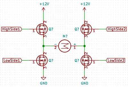
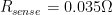 , and an INA240 current sense amplifier with a gain of 50. Why these values? Two competing objectives:

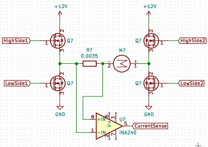
 resistors are gate resistors. We put them here because the driver is very powerful, and if we don’t have any resistance here, it will draw huge current spikes at every switch to charge and discharge the MOSFET gates. We slow it down a bit with these resistors to keep our supply rails a bit cleaner. What specific values to use is a bit more complicated – first we have to figure out how fast we need the FET to switch, and then look at the MOSFET’s gate capacitance, and use that to figure out the maximum gate resistance we can put in. If you are interested in how this works, see the end of