Building an ESP32 Light Controller
In this post I am going to do a deep dive into the electronics design for my simulated sunrise/sunset aquarium light project. If you have not read that post, I recommend starting with that.
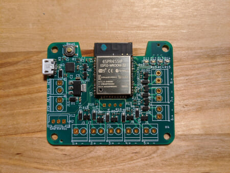
The victim
Disclosure: JLCPCB is sponsoring my projects, but I had already been a big fan of their PCB manufacturing/assembly services for a long time before that, and can recommend them without reservation.
Requirements
- 12V power
- Control 8x 12V lights at up to 1A each, with PWM at <= 20 kHz
- WiFi for time sync and remote override
- As small as I can make it so it doesn’t become an eyesore on my fish tank
Design
Main Controller
I am using the ESP32-WROOM-32 module for this project. It’s got a dual core 240 MHz 32-bit Xtensa CPU with an integrated WiFi controller. The module integrates all the external components required for the ESP32 chip – flash, crystal, and high frequency decoupling, as well as an impedance matching network and a MIFA PCB antenna. At about £3 (~US$4) each from Digi-Key, it’s also incredibly inexpensive for what you get.
Why? WiFi. Most of my IoT devices already run on WiFi, so using another standard would require getting another hub, and except in very low power designs and devices that need very long range, WiFi is a good choice for convenience (both in hardware and software setup), and data rate.
I can go with something like TI CC3000 with a separate controller, but since my microcontroller needs in this project are very modest (just PWMing 8 MOSFETs!), it’s easier and cheaper to just use the ESP32.
The circuit is basically a copy of the example circuit supplied in the datasheet. There’s really not much to it:
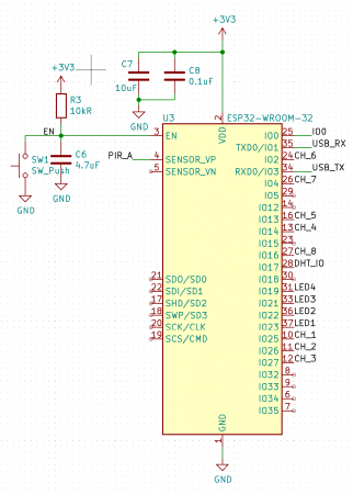
ESP32 circuit
Integrated USB->UART bridge
The ESP32 is programmed over UART, and I can either break out a UART header to attach an adapter cable to, or integrate a bridge IC so I can just use USB. Using a separate adapter is cheaper because I only need one of those, but the Silicon Labs CP2104 is $1.29 from JLC. I went for the convenience of only having to plug in a USB cable.
The CH340G is an even cheaper ($0.36) option from a Chinese company, but I wasn’t too worried about cost since I am only making a few of these, and I have successfully used CP2104 before. The CH340G also requires a crystal, which means larger board area, and of course you have to pay for the crystal (and compensation capacitors for the crystal). It’s also in SOIC instead of QFN. I didn’t think I would ever come to prefer QFN over SOIC when I was hand soldering my boards, but now that JLC is soldering them, the space savings with QFN is great!
The circuit is, again, mostly just a copy of the recommended application circuit in the datasheet.
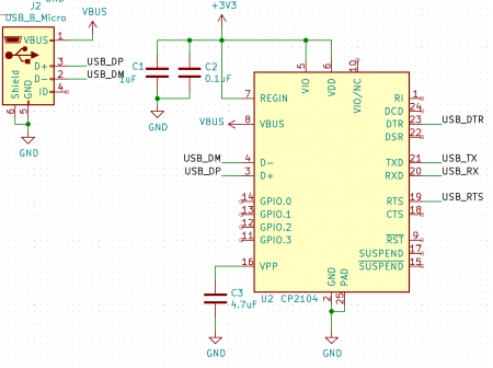
USB circuit
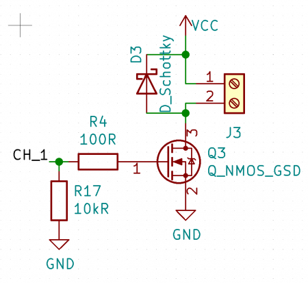
MOSFET Choice
This board needs to do one thing – switch lights on and off (very quickly). If it can’t do that one thing well… I’d be sad. The choice of the MOSFET is crucial. I want to be able to pass 1A, and support up to 20 kHz PWM. We can often get away with a lower frequency, but there’s always the possibility of audible resonance, which is very annoying and impossible to predict, and can be solved by taking PWM frequency above audible range (20 kHz). So whenever possible, it’s a good idea to design the hardware for 20 kHz, and lower it to reduce switching losses if possible. I did end up running into the noise problem on this board, and had to run PWM at 20 kHz.
I know my requirements are modest, so I am primarily optimising for space and cost.
JLC doesn’t have the best parts search interface, but here are the basic MOSFET options:
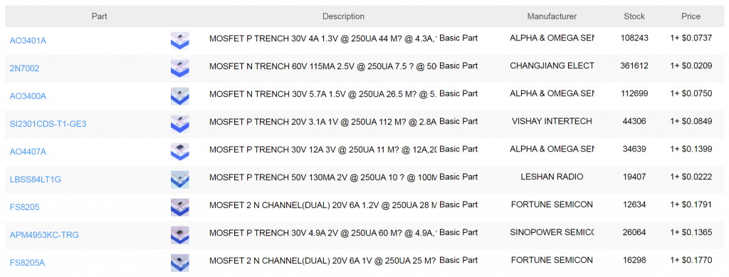
I wanted something that’s a “basic part” because those are the parts already loaded on their pick and place machine, and don’t require an additional charge. They charge $3 for each type of extended part used.
Looking at the single N-channel MOSFETs, our choices are 2N7002 (not suitable because it’s a small signal MOSFET – designed to be fast but can’t take much current), and AO3400A.
As it turned out, the AO3400A is perfect. It’s tiny (SOT23 package), has an Rds(on) of 48 mΩ even with only 2.5V Vgs, and a maximum drain current of 5.7A (at Vgs=10).
I decided to drive the FET with ESP32 digital output instead of using a MOSFET driver. This is a somewhat risky thing to do, for two reasons –
- We will only be driving the gate with 3.3V, and MOSFETs can pass more current and with a lower on state resistance when the gate is driven to a higher voltage.
- The current output of a microcontroller digital pin is limited, which means we may not switch the MOSFET on/off fast enough (that requires charging/discharging the gate charge).
So we have to do the math to prove to ourselves that it will be fine. We start with the datasheet.
First thing is to verify that we are below the absolute maximum Vds rating. That’s 30V here, and we are fine.
Then we look at how “turned on” the MOSFET will be at 3.3V.
Figure 1 (Id vs Vds) tells us all we need to know.
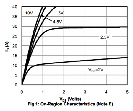
Id vs Vds
It gives us Id vs Vds plots for different Vgs options. Ideally we want the MOSFET to behave like a resistor when on, and that means we want to stay in the saturation region, and not the later linear region, where increasing voltage over the MOSFET does not result in higher current flow (ie. it’s no longer behaving like a resistor).
It does not have a plot for 3.3V, so we go down to the next conservative option, which is 3V in this case (because we know that the MOSFET will be “more on” at 3.3V than 3V). We see that it’s totally linear until about 30A, and that’s way more than plenty (remember that we only need 1A).
We can also work out the Rds(on) from the slope of the linear region, but it’s easier to consult another graph –
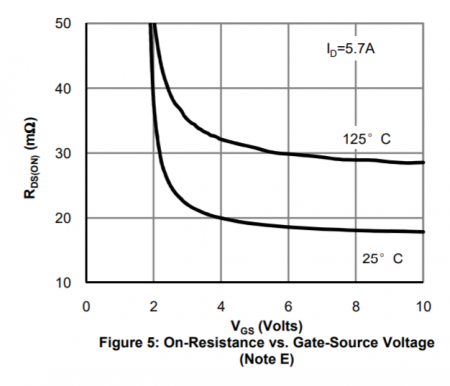
Rds(on) vs Vgs
Here we see that for Vgs = 3.3V, we are looking at about 22 mΩ at 25C, and about 35 mΩ at 125C. I know this circuit will mostly be kept around room temperature, so I’ll use 25 mΩ.
Now we can calculate power dissipation in the MOSFET in on state –
P = I^2 * R, for I = 1A, and R = 0.025Ω. We get P = 0.025W. This MOSFET won’t even get warm!
With power dissipation out of the way, let’s look at how fast we can switch the thing, and that involves looking at the various parasitic capacitances that affect the gate, because we have to charge and discharge them every time. Now there are much more complicated models available because MOSFET gates don’t actually have constant capacitance (if components that have constant resistance is called ohmic, can we call this non-faradian?). This is due to the Miller effect. You can learn all about that in this nice tutorial from Microsemi if you are interested. But unless we are working very close to the limit, we can use a vastly simplified model – total gate charge (Qg), which is the total charge that needs to be injected into the gate, divided by Vgs gives us the gate capacitance, and we just think about charging/discharging that capacitance.
Figure 7 tells us what we need to know:
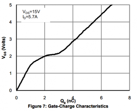
Vgs vs Qg
Here we see that at Vgs = 3.3V, we get a gate charge of about 5nC, which means a gate capacitance of about 1.5nF. Notice that this is tested at Vds = 15V and Id = 5.7A, which is not quite how we will be operating the FET. We have a lower Vds (12V), and a lower Id (1A), so our actual Qg won’t be exactly the same as in the figure. Generally speaking, a lower Id increases gate charge, and a lower Vds reduces it. This would be something to look into if we get close to the limit. We’ll use the value straight from the figure for now. In practice, if I am getting close to the limit, I will just add a gate driver instead for the peace of mind. My go-to chip for this is the MCP1416. It’s tiny, cheap, has a very wide operating voltage range, gives me a nice 1.5A gate drive, and is very easy to use.
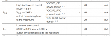
How fast can we charge it? The ESP32 datasheet says we can source 40mA, and sink 28mA before the output voltage changes significantly (from 3.3V to 2.64V and 0V to 0.495V).
Ioh and Iol
For simplicity we will use a 100Ω gate resistor, which would limit the current to about 33mA (3.3V / 100Ω). So now we need to figure out how fast we can charge a 1.5nF capacitance through a 100Ω resistance, and this is an application of the basic exponential capacitor charging equation, where the time constant τ = RC. That’s 150 nanoseconds in this case, to charge to 63.2% of the final value, and and 300 nanoseconds (two time constants) to charge to 86.5%. That’s a good enough approximation of the rise/fall time for our purposes.
Remember that we were aiming for a PWM frequency of 20 kHz, which has a period of 50 microseconds. In general, we want the rise and fall time to be less than 1/10 of the period, or 5 microseconds in this case. We are plenty fast enough. In fact, we are good for up to about 300 kHz, but there’s really no point going above 20 kHz.
At $0.075/FET, looks like we have a winner! This is a very impressive MOSFET. Low Qg vs low Rds(on) is the major tradeoff in MOSFET design, and usually you can’t have both. This FET seems to have done the impossible, and I don’t think FETs like these existed say 20 years ago.
The circuit. We also added a pull-down resistor to make sure the FET is off at power on, before the microcontroller starts controlling the gate. I also have a flyback diode. That’s probably not necessary in this case, because lights are not typically inductive, but I’m thinking I may want to re-purpose this board to drive motors or solenoids later on, and the diodes are only $0.03 each, and someone else is soldering them.
Power Supply
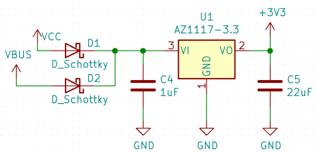
Power supply circuit
Here we have the power supply. The two Schottky diodes allow for two sources of power – 12V main supply or 5V USB Vbus (which ever is higher will supply the current). This allows me to program and debug the board without 12V power connected.
I am using a linear regulator, which is horribly inefficient going from 12V to 3.3V, but we are drawing less than 100mA at 3.3V, and the lights are drawing about 4A total. Insignificant at the end of the day.
The only decisions to make here are the input and output capacitors. Followed what the datasheet recommends. Very important for the stability of many regulators.
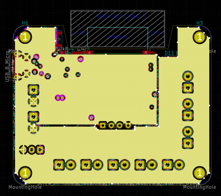
PCB
And finally we get to the PCB design. I designed this as a 4 layer board to minimise size. As an aside, I almost never make 2 layer boards anymore. JLC can make 5x 100mm by 100mm 4 layer boards for $7. Why make my life more difficult trying to route this on 2 layers (and suffer worse signal integrity)? My time is worth a lot more than the $5 that would be saved (they charge $2 for 2 layer of the same size).
The ground plane first:
Ground plane
The middle section is for the ESP32, and the outer ring has the load-switching MOSFETs (which handle the return current from the loads). This is a star grounding design to prevent load return current (which is on the order of 4A – very high for the size of the plane) from passing under the ESP32 and introducing ground noise there.
The power plane looks similar:
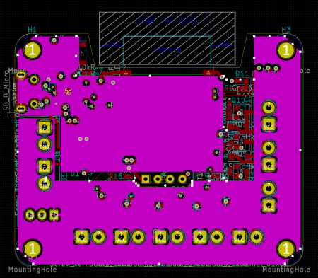
Power plane
But the two parts of the plane aren’t connected. The inner part is for 3.3V, and the outer part of 12V.
And finally the signal layers:
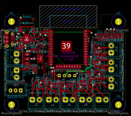
Signal layers
This is quite dense routing, but pretty straight forward. I used it as an exercise to see how small I can make things, and most of the 50x60mm board is taken up by connectors. All the passives are 0402. Hey, someone else is soldering them!
Assemble and Test
A few days later, I got the boards in the mail from JLC, and soldered the connectors, ESP module, and the USB port myself.
(Almost) assembled
Does it work? Yes!
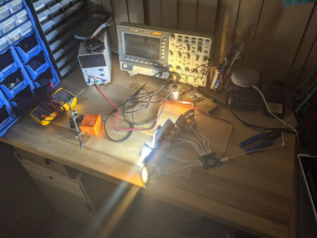
Tested
How about the MOSFET gate rise time that we spent so much time calculating?
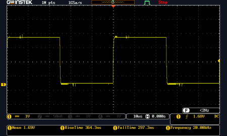
PWM scope shot
Beautiful waveform at 20 kHz. 364ns rise time and 297ns fall time. Almost exactly what we calculated, even though we used a vastly simplified model that would have driven a power systems engineer bananas.
And just for fun, this is what the waveform looks like if the edges are too slow for the frequency. This is at 500 kHz.
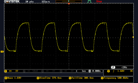
500 kHz PWM
Here we see that the rise and fall times take up significant portion of the period, which means the FET will spend a lot of time in the saturation region, where they are partially on. We want the MOSFETs to be in fully on (aka triode or linear region) or fully off (aka cutoff) regions as much as possible, since there is very little power dissipation in both.
P = VI. When the FET is fully on, the voltage is very low (0 for an ideal FET). When the FET is fully off, the current is very low (0 for an ideal FET). During transition is the only time where there is a significant voltage drop across the FET as well as a significant current passing through it.
I like to look at all my boards with an infrared camera to see if anything is unexpectedly hot.
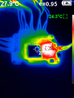
IR image
The MOSFETs are not heating up at all, even after extended operation. Of course, we knew that already from the calculations. The regulator, on the other hand, is getting quite toasty.
You can see the whole system in operation in the video at the beginning of the original post.
Files
All files below are hereby released under CC BY-SA.
KiCad: https://github.com/matthewlai/WiredHut/tree/master/hardware/light_control/light_control