Designing with USB-C: Lessons Learned
I spent hours reading the USB-C spec so you don’t have to. A guide to designing compliant circuits with USB-C for hobbyists.
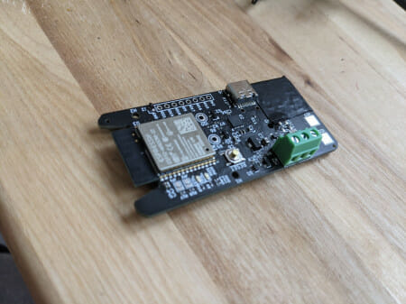
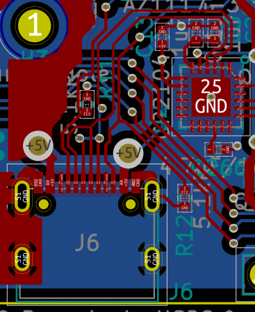
My first USB-C design!
Disclosure: JLCPCB sponsors some of my projects, but I would never recommend something that I wouldn’t otherwise. Their SMT Assembly service I believe is unique in the industry, and is great for hobbyists who need high quality assembled prototypes for cheap, without having to deal with logistics of component supply.
TLDR: Scroll to the “Putting It All Together” section. Implement that circuit, and use it like a good old Type B port.
Introduction and History
USB is really a miracle connector. I have been designing PCBs for about a decade now (mostly as a hobbyist due to selling out and joining the software world for my career after my EE degree), and of the dozens of boards I’ve designed, I can probably count on one hand all the designs without a USB port.
Why do I put a USB port on virtually all my boards? Because it:
- Supplies power at a convenient voltage.
- Most of the microcontrollers I use nowadays have either a serial bootloader (ESP32) or built-in USB DFU bootloader (STM32), so it can be used to program the chip.
- A serial port for debugging (either through a USB-UART chip or enumerating as a CDC-ACM virtual serial port in firmware for STM32).
What more can you ask from an ubiquitous connector that takes up minimal board space, and uses cables you can buy from even grocery stores? If you want to power your project with a wall wart, USB chargers are readily available, too (even from grocery stores).
But wait, it gets even better. Back in 2014, the USB-C standard was finalised, and Google was the first major manufacturer to adopt it with the 2015 Chromebook Pixel, with Apple following shortly after with the 2015 MacBook. Initial adoption was a bit slow, but over the past few years, USB-C has taken over the consumer electronics market, and most laptops and smartphones come with USB-C nowadays. That’s a very good thing, because USB-B had many pain points –
- USB was not designed to supply significant amount of power initially – only 5V @ 500mA. As a result, to support battery charging, manufacturers started adding proprietary extensions for higher current (and sometimes voltage) – Qualcomm’s Quick Charge, Sony had their own thing, Apple had their own thing, and Samsung had their own thing. None of them were inter-operable, making designing a “universal” power sink very challenging. Eventually USB-IF (the governing body of USB) came up with the Battery Charging Specification (BCS), but it was a bit too late, and it’s also unnecessarily complicated due to having to make do with the existing data pins. It must not break existing devices that don’t understand BCS, and in designs where we need both high current and data transfer, having to multiplex BCS detection circuitry with data lines is always a pain. It’s also limited to only [email protected], because A-B cables don’t have any identification mechanism, and burning down a user’s house trying to push 5A through a cable designed for 1.5A is frowned upon.
- Different connectors for USB 1.1/2.0 and 3.0.
- Different connectors for host vs device. The initial design calls for USB-A ports on hosts, USB-B ports on devices, with a few size variations for both (mini and micro – they are electrically identical to full fat versions… more or less). It made sense – if all hosts have Type A ports, all devices have Type B ports, and we only make A-B cables, everything works as long as they fit! … Well, until we realised that we want some things to be devices some of the time, and hosts some of the time – phones and tablets. They need to be device when charging or plugged into a computer, but host when we want them to read a USB flash drive or use a USB keyboard to write a long blog post. So like BCS, we bolted it on with the USB OTG abomination, which also left a lot to be desired.
- USB superposition.
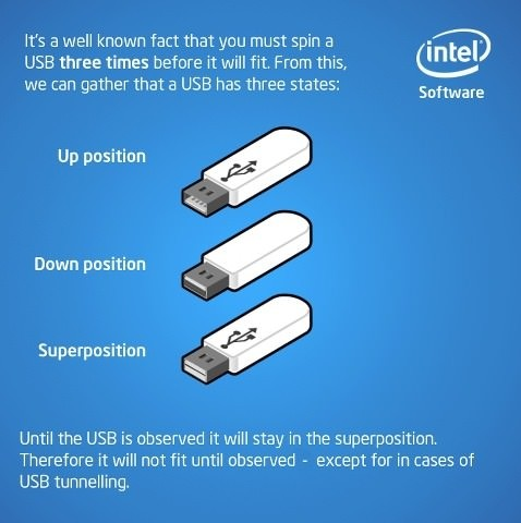
USB Superposition
USB-C solved all those problems from the ground up:
- We can now get up to 5V@3A with a very simple detection mechanism that just requires 2 ADC pins, or 1 if we add a bit of additional hardware. No complicated multiplexing needed because they are not on data pins. If we want higher voltage/current, we can get up to 20V@5A with the new Type C Power Delivery standard though that is more complicated. Best of all, this is all standardised. Nothing is proprietary, and all USB-C devices support these (ok, maybe that’s optimistic… let’s just say all devices from reputable manufacturers do).
- One connector rules them all – USB 1.1/2.0, 3.0/3.1/3.2, 4.0, even DP, HDMI, audio, and a few other things.
- One cable rules them all – C to C is all we need (ok that’s a lie, we actually have two types of cables, one basic type for up to USB 2.0 @ 3A, and a fancier type that self-identifies their capabilities). Roles are determined electrically, not using connectors.
- No more superposition!!
Despite being a big fan of Type C from the early days, I have only just designed my first PCB with USB-C, in 2021, feeling like a hypocrite this whole time buying only USB-C devices, and still making micro-B ones!
Why? Mostly because Type-C connectors tend to be much harder to solder (much more pins, about the same total connector size). The standard is also much more complicated, though as we will see shortly, actual implementation is VERY simple if we just want to use it to replace micro-B in USB 2.0 devices (as opposed to hosts).
What changed? Well, JLCPCB started offering Type C connectors with their SMT assembly service, so I have no excuse now!
I did a lot of reading up on Type C for my first project, both official and unofficial sources, and I thought I would write a post summarising all I have learned and de-mystify it a bit, and hopefully encourage other hobbyists/makers to adopt USB-C.
Scope
Type C is a very big standard. The “bible” – Universal Serial Bus Type-C Cable and Connector Specification, is 373 pages long. They clearly learned from their mistake before, and decided to include EVERYTHING that anyone can conceivably need into the standard. But for basic applications, you don’t actually need to know all those things. You should (if I do my job) be able to use Type-C as a micro-B replacement in a standard-compliant way by just reading this post.
I’ll limit the discussion in this post to designing Type-C pure devices (called upstream-facing port or UFP in the spec), pure power sinks (USB-C actually allows devices to negotiate switching power supply direction without switching data host/device!), and communicate at up to USB 2.0 HighSpeed. This I think encompasses most hobbyist applications.
Let’s get started.
Connectors
This is the connector pinout from Wikipedia:
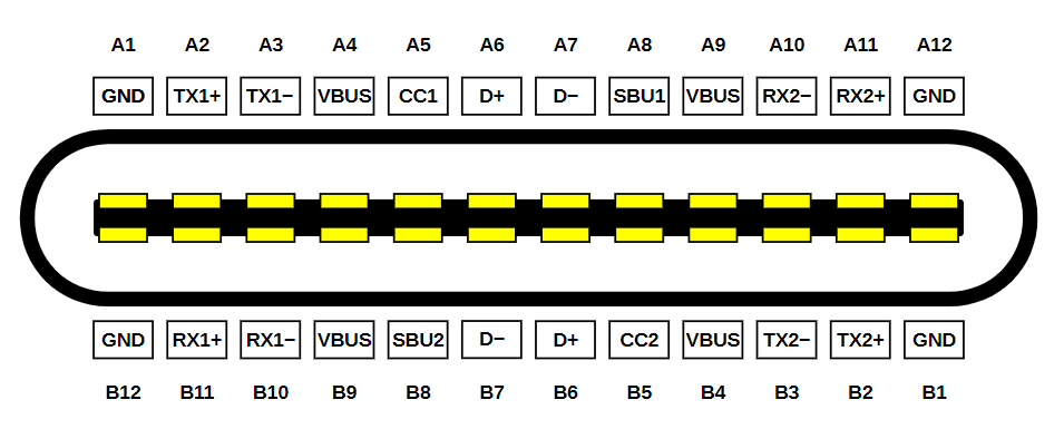
USB-C Connector Pinout (By Chindi.ap, CC BY-SA 4.0, Wikipedia)
It looks quite daunting, but we actually don’t care about most of those pins for our application:
- TXn+, TXn-, RXn+, RXn- pins are for USB 3 SuperSpeed, so we can ignore them.
- SBU1/2 pins are for side band use (used for low speed communication when the port is used for something like DP or HDMI), so we can also ignore them.
That leaves us with these pins –
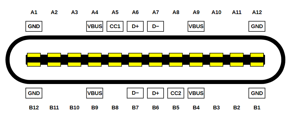
Simplified USB-C Connector Pinout
Much more manageable. Most of them are pins we already know and love – VBUS, D+, D-, GND. Except they are all doubled/quadrupled now to support reversible insertion. They can (and should) all be shorted together.
The only new pins are CC1 and CC2 (channel configuration), and they do a few things:
- Pull down resistors on the device side tells the host that a connection has been made with a device, and VBUS should be turned on. Unlike Type A, in Type C VBUS is never energised until a host knows a device is there, because the user may plug two hosts into each other, and terrible things would happen if they are permanently live.
- On the device side, one of them will read as ground, and the other some higher voltage. This tells us the cable orientation. It’s important for 3.0/SuperSpeed operations, but we don’t actually care about orientation for 2.0, since we are shorting all the other pins together! I will refer to the non-ground one as CC from now on, though it can be physically on either CC1 or CC2 depending on orientation (and we must account for both possibilities, otherwise our device will only work with cable inserted one way). No, we cannot short them.
- The CC voltage is used to determine how much current is available from the upstream port, and whether there is a connection. This voltage is determined by a voltage divider between host and device.
- If we want to do Power Delivery (we need more than 5V@3A), the communication also happens on the CC pin, but it’s much more involved and we probably want to use a PD sink controller to handle that for us (eg. ST STUSB4500).
The standard requires that CC1 and CC2 be pulled down to ground on the device side with a 5.1k ±10% Ω resistor each (Table 4-25 in the spec), and with a basic C-C cable, only one will be connected to the host, which will have different valued pull-up resistors to indicate how much current it can supply – 56kΩ, 22kΩ, or 10kΩ to 5V, or an equivalent current source, or equivalent pull-ups to 3.3V (Table 4-24).
So in the end, the whole circuit looks like this:
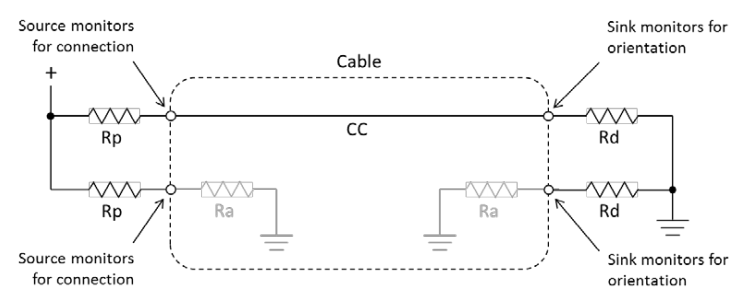
Connectors + cables circuit (Silicon Labs)
In a basic USB 2.0 3A cable, Ra doesn’t exist, but fancy cables that support higher speeds or higher currents will have them to power electronics in the cable so they can tell the host their capabilities. On the device side we don’t care about that, but that’s the reason why we can’t short the CC pins and just use one resistor. Raspberry Pi Foundation did that with early revisions of the Raspberry Pi 4, and it didn’t end well for them. Don’t be like them.
In terms of determining how much current you can draw, just read the CC voltage (remember that it’s the higher of CC1 and CC2). Thresholds are as follows:
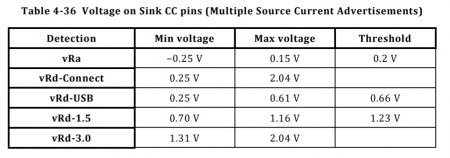
Table 4-36: Current advertisement
So what that means is:
- [0V – 0.2V]: No connection (we only care about this if the device is self-powered, because in a bus-powered device, the fact that we have power and the firmware is running means there is a connection)
- [0.2V – 0.66V]: Standard USB current available (the host either has no high current capability, or we are connected to a legacy host with a A-C cable – see “How Much Current Can I Draw?” for more details)
- [0.66V – 1.23V]: 1.5A available
- [1.23V+]: 3.0A available
In practice, most laptops will supply 1.5A or 3.0A, most wall warts will supply 3.0A, and phones (if we use them as host) will support standard USB. The CC voltage may change over time and should be continually monitored. When it changes, the device has 60ms to be compliant with the new advertised current limit (tSinkAdj, Table 4-29).
If we are using a USB-A power supply with an A-C cable, it will always show vRd-USB because the pull-ups are actually inside the cable, since a USB-A host knows nothing about CC signals, and a compliant A-C cable can’t assume the host can supply more. There ARE non-compliant cables that do advertise high current support to device without checking with host. They are a fire risk and should never be used. Fortunately they are less common now in 2021. So if we want to draw more current from a legacy power supply, we have to go back to the pre-Type-C madness on data lines.
Putting It All Together (aka TLDR)
With that, we arrive at the schematics for using a Type C port as a micro-B replacement –
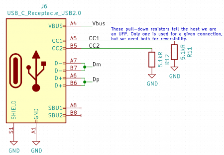
Simple Type C schematic
Vbus, D+, D-, and Gnd are used just like in legacy connectors.
CC1 and CC2 must have a 5.1kΩ pull-down each. If you want to take advantage of the new Type C current advertisement mechanism, they should be routed to ADC pins on your microcontroller, but if you don’t need that, leaving them alone with just the pull-downs is perfectly fine, too, and it will act just like a standard Type B port electrically.
Note that I am using a connector with only the USB 2.0 pins. If you are using a fully-featured connector, all other pins can be left unconnected.
Choosing a Connector
Now that we have decided to add USB-C to our project, we need to pick a connector to use. It’s not easy – there is a huge variety on the market, and some are much harder to use than others. Generally, they are one of these four types.
Full Featured All SMT
First type is a fully featured connector with two rows of SMT pads. They are probably the most difficult to use for hobbyists, because there is no way to inspect/fix the inner pads, and at ~0.3mm pitch, those pads are very close together, and may short if your reflow process isn’t absolutely perfect.
If you are getting your boards professionally assembled, this may be ok, but there’s no need to risk it if you don’t need USB 3.0 SuperSpeed.
Here is one example: Korean Hroparts TYPE-C-31-M-05.
Full featured connector
Full Featured 1/2 SMT 1/2 TH
And then we have connectors where the back row uses through-hole pins instead of pads. They are probably easier, but the pins are very close together, and it seems like a huge hassle.
Example: JAE DX07S024XA8R700.
JAE DX07S024XA8R700
USB 2.0-Only SMT
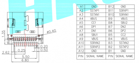
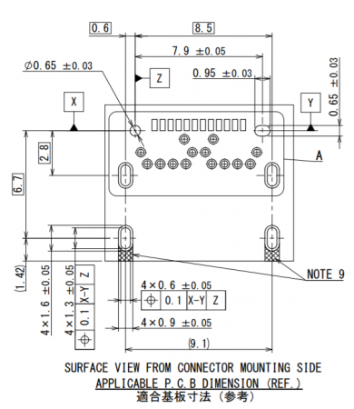
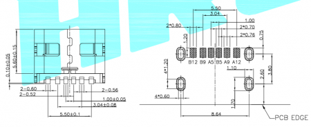
And then we have connectors that omit all the pins not required for USB 2.0, and we end up with a connector with just one row of SMD pads, with reasonable spacing. This option I believe works the best for our applications, and my chosen connector is the Korean Hroparts TYPE-C-31-M-12 (LCSC part number C165948).
JLC has a lot of them in stock as of this writing, and offers them for $0.307 at qty 1, and a few cents to solder them for us.
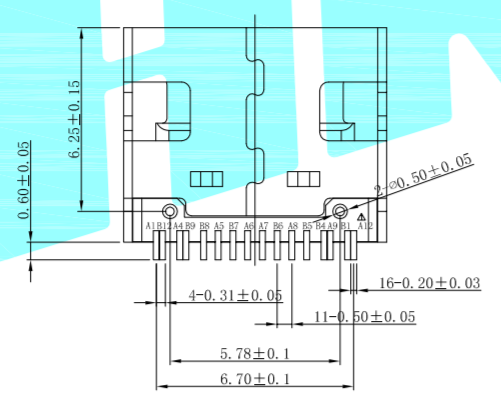
Korean Hroparts TYPE-C-31-M-12
It has worked very well for me so far – perfect assembly quality from JLC, using KiCad’s built-in footprint for this connector.
I have never had to solder it myself, but because the pins actually extend past the housing (unlike many micro-B connectors), I feel this is probably pretty easy to hand-solder, too, if you are used to soldering QFPs.
Power-Only SMT
If we don’t need data transfer at all, there are even simpler connectors that only have power and the CC pins (so we can determine how much current we can draw). I have not tried them.
Example: Korean Hroparts TYPE-C-31-M-17. It’s $0.191 from JLC, so you save about 11 cents.
Korean Hroparts TYPE-C-31-M-17
How Much Current Can I Draw?
Continuous
If you have a USB-C power supply, just read the CC voltage, and refer to Table 4-36 copied above. If you want to support legacy power supplies as well with A-C cables, you also have to implement detection based on Battery Charging Specification 1.2.
Maxim has a guide on how to do that: https://pdfserv.maximintegrated.com/en/an/TUT5801.pdf
But it basically boils down to this (as I understand it) – there are 3 types of ports. Standard Downstream Port (SDP) which is data only with no high current capacity, a Charging Downstream Port (CDP) which is data + 1.5A, and a Dedicated Charging Port (DCP) which is 1.5A with no data.
One possible detection algorithm is to apply 3.3V to D+, and read D-. If it’s 3.3V, we have either CDP or DCP (otherwise SDP). Then we do the same, but reversed (apply voltage to D- and read D+). If D+ reads 3.3V, we have a bi-directional short between D+ and D-, which means we have a DCP. Otherwise it’s a CDP.
And remember that you have to multiplex it with data, if you also want to do data transfer.
If you want to support proprietary implementations, that’s a whole nother can of worms. Both Apple and Sony use resistive dividers on data lines that can be read with an ADC. Quick Charge I believe requires a dedicated controller.
Without either CC showing 1.5A/3A or BCS showing CDP or DCP, we have standard USB current, and that’s a lot more complicated. In this case you are allowed to draw 500mA only if your device cannot enumerate. If your device does enumerate, it must draw maximum of 100mA until negotiated otherwise with the host as part of the enumeration process (up to 500mA).
Startup Current
So either Type C current advertisement or BCS tells us the maximum continuous current, but what about peak current at plug-in, when all the capacitances charge up?
The spec allows for 10µF on Vbus (Table 4-3: VBus Sink Characteristics) or equivalent. What that means exactly is not 100% clear, but most people take it to mean that the initial current spike above the max continuous current allowed, when integrated over time, should be no more than 50µC, which is what a 10µF capacitor will draw at 5V. So if we have a huge capacitor behind a regulator, that would count, too, unless our regulator is current-limiting.
It does NOT mean we can’t have more capacitance than that. What that means is if we have more capacitance, we have to limit the inrush current so that they don’t appear as “naked” capacitance on Vbus (it may trigger overcurrent reset from the host). If we limit the charging speed of our capacitance to the max continuous current, we can have as much capacitance as we want.
Fortunately, there are many chips (usually called USB Power Distribution Switches) that can handle this for us. For example, the Diodes Incorporated AP2162/2172.
Current Slew Rate
This one is a bit harder to design for, and is probably more practically verified on the prototype rather than ensured by design. The maximum current slew rate (dI/dt) is 150mA/us, both on ramp up and down. This is the iLoadStepRate(max) in the spec, and the reason why it’s limited is because too much dI/dt can cause unacceptable Vbus voltage drop on the host due to inductance in the power supply path. If your design is exceeding this, it needs more capacitance (potentially requiring the use of a current-limiting switch, as described above).
Suspend Mode
A compliant device must implement suspend mode. In short, if there is no traffic on the data bus for 3ms, the device has 7ms to enter suspend mode where it must draw no more than 2.5mA. This may be difficult to implement if you don’t do USB yourself, but for example, the Silicon Labs CP210x USB-UART chip has SUSPEND outputs for this purpose. The microcontroller can monitor it, and turn into go into sleep mode if/when it goes high.
This requirement may be ignored if either CC indicates 1.5A/3.0A, or the host is a CDP/DCP port as detected through BCS.
PCB Design
PCB Design
It depends on what connector you choose, but in my case it’s pretty simple. All the shorting does make it a bit more complicated, but still easily doable on 2 layers, which is a requirement for this project due to cost-sensitivity (most of my other projects are 4 layers now).
For routing the data traces, standard rules apply (this is not specific to USB-C). They should be routed close together, with minimal vias and parallel runs of traces on another layer. Do we need impedance-controlled routing? Well, if you have a 4 layers board and you get free impedance control from your fab (like JLC), might as well do it. But whether that’s necessary or not depends on speed (edge rate) and trace length.
The general rule of thumb is if the edge rate divided by signal travel time is smaller than 6, we need to think about treating it as a transmission line (with controlled impedance).
USB minimum edge rates are 75ns for Low Speed, 20ns for Full Speed, and 500ps for High Speed. That gives us a maximum propagation time of 12.5ns, 3.33ns, and 83ps respectively. Velocity of propagation is ~0.6c, which gives us a maximum trace lengths of 2.2m, 60cm, and 1.49cm respectively, without having to worry about transmission line effects. In practice that means we don’t really need to worry unless we are doing High Speed (or we have very long traces).
So what if we need controlled impedance? We have to calculate the trace width and spacing, based on the dielectric our fab is using. For example, this is JLC’s calculator. USB spec requires differential impedance to be 90Ω, which means that given a trace space of 5 mil (that’s a free parameter), we need 8.1 mil traces with the JLC7628 dielectric, or 5.17 mil traces with the JLC2313 dielectric. Using their standard stackup for 4 layers 1.6mm boards.
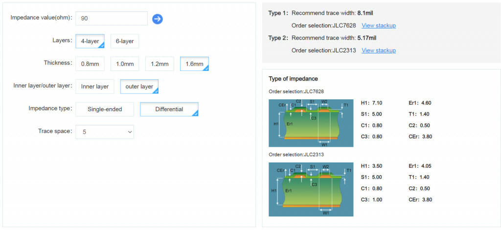
Impedance calculator
Your result will be different depending on the fab, dielectric, and the stackup they use. There should always be a solid ground plane underneath the transmission line, and no other trace should be within 3x the width of the traces.
CC lines are low speed, and you can do whatever you want with them (within reason…).
Good luck with your designs and hope we will soon be in USB-C-opia!
Discussions on Reddit: https://www.reddit.com/r/diyelectronics/comments/mlyedi/guide_to_designing_with_usbc/